
User`s guide


Interfacing DDR2 and DDR3 Memories with the i.MX53 Processor
i.MX53 System Development User’s Guide, Rev. 1
6-10 Freescale Semiconductor
setmem /32 0x63fd901c = 0x092080b0 //write mode reg MR0 with cs0 , with dll_rst0
setmem /32 0x63fd901c = 0x04008040 //ZQ calibration with cs0 (A10 high indicates ZQ cal long
ZQCL)
//**********************************
// CS1:
//**********************************
setmem /32 0x63fd901c = 0x0000803a //write mode reg MR2 with cs1 .
setmem /32 0x63fd901c = 0x0000803b //write mode reg MR3 with cs1
setmem /32 0x63fd901c = 0x00028039 //write mode reg MR1 with cs1. ODS=01: out buff= RZQ/7
setmem /32 0x63fd901c = 0x09208138 //write mode reg MR0 with cs1
setmem /32 0x63fd901c = 0x04008048 //ZQ calibration with cs1 (A10 high indicates ZQ cal long
ZQCL)
//**********************************
setmem /32 0x63fd9020 = 0x00001800 // Refresh control register
setmem /32 0x63fd9040 = 0x04b80003 // ZQ HW control
setmem /32 0x63fd9058 = 0x00022227 // ODT control register
setmem /32 0x63fd901c = 0x00000000
// CLKO muxing (comment out for now till needed to avoid conflicts with intended usage of
signals)
//setmem /32 0x53FA8314 = 0
//setmem /32 0x53FA8320 = 0x4
//setmem /32 0x53FD4060 = 0x01e900f0
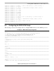
6.5 Configuring the i.MX53 Registers for the Initialization Script
This section explains how to configure the registers of the i.MX53 for the initialization script, using
values taken from the Micron MT41J128M16-187E memory data sheet as the example. Therefore, in this
example CK = 2.5 ns.
6.5.1 Main Control Register
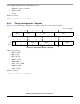
Figure 6-4 shows the main control register’s bit fields, access, and reset values.
The memory values are as follows:
• ROW = 14
• COL = 10
DDR3 only supports a burst length of 8. Therefore, BL = 8 burst length.
Access: Read/Write
31 30 29 27 26 24 23 22 21 20 19 18 17 16 15 0
R
SDE_0 SDE_1 — ROW — COL BL — DSIZ —
W
Reset 0 0 0 0 0 0 1 1 0 0 0 1 0 0 0 1 0000000000000000
Figure 6-4. Main Control Register