
User`s guide

i.MX53 System Development User’s Guide, Rev. 1
Freescale Semiconductor 6-1
Chapter 6
Interfacing DDR2 and DDR3 Memories with the i.MX53
Processor
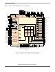
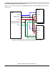
This chapter explains the interface between the i.MX53 processor and DDR2 and DDR3 memories. It
includes the routing guidelines, pictures, and examples.
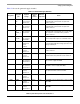
6.1 i.MX53 SDRAM Controller Signals
The SDRAM controller can be interfaced with LPDDR2-S, DDR2, and DDR3 memories. The DDR
controller from the i.MX53 uses the following signals to interface the memories:
• Data bus and its buffer control signals
— DRAM_D0 – DRAM_D31.
— DRAM_DQS0/DQS0_B - DRAM_DQS3/DQS3_B.
— DRAM_DQM0 – DRAM_DQM3.
• Address bus and its bank control signals
— DRAM_A0- DRAM_A15
— DRAM_SDBA0- DRAM_SDBA2
• Control
— DRAM_RAS
—DRAM_CAS
—DRAM_SDWE
—DRAM_RESET
— DRAM_CALIBRATION
— DRAM_SDCKE0 - DRAM_SDCKE1
— DRAM_CS0 – DRAM_CS1
— DRAM_SDODT0 – DRAM_SDODT1
•Clock
— DRAM_SDCLK_0
— DRAM_SDCLK_0_B
— DRAM_SDCLK_1
— DRAM_SDCLK_1_B