
User`s guide


Setting up Power Management
i.MX53 System Development User’s Guide, Rev. 1
5-12 Freescale Semiconductor
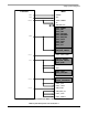
5.5 Connecting Power and Communication Signals
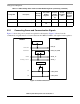
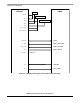
Figure 5-7–Figure 5-10 show the required connections for interfacing LTC3589-1 and LT3481 with the
i.MX53. Both power domains and communication signals blocks are specified for a more complete
understanding of the interface.
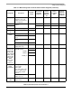
Figure 5-7. Power Connections Block (LT3481)
NVCC_RESET LVIO 1.8 or
2.775
Note 1 1.8 125 2
USB_H1_
VDDA25
USB_OTG_
VDDA25
NVCC_XTAL
USB_PHY analog supply,
oscillator amplifier analog
supply
2.5 SW3 2.5 1200 2
USB_H1_
VDDA33
USB_OTG_
VDDA33
USB PHY I/O analog
supply
3.3 SW4 3.3 1200 4
VDD_REG Power supply input for the
integrated linear
regulators
2.5 SW3 2.5 1200 2
VP SATA PHY Core power
supply
1.3 LDO2 1.3 250 3
VPH SATA PHY I/O supply
voltage
2.5 SW3 2.5 1200 2
1
These domains are supplied by the internal regulator of the i.MX at the VDD_ANA_PLL pin.
2
An external DCDC converter is needed to supply these domains.
3
External part regulator number is LT3481.
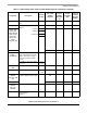
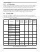
Table 5-2. i.MX53 Voltage Rails and Associated LTC3589-1 Regulator (continued)
Voltage Rail Description
Nominal
Voltage
Associated
LTC3589-1
Regulator
Voltage Set
Point of
LTC3589-1
Regulator
(V)
Current
Capability
(mA)
Power up
Sequence
Set at the
LTC3589-1
LT3481
i.MX53
NVCC_EIM_DRAM
SW