
User`s guide
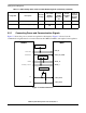
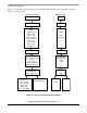
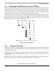

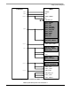

Setting up Power Management
i.MX53 System Development User’s Guide, Rev. 1
Freescale Semiconductor 5-11
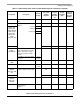
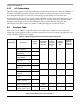
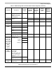
NVCC_CKIH ESD protection of the
CKIH pins, Fuse read
supply and 1.8 V bias for
the UHVIO pads
1.8 Note 1 1.8 125 2
NVCC_LCD GPIO digital power
supplies
1.8 or 2.775 LDO3 2.8 250 3
NVCC_JTAG LDO3 2.8 250 3
NVCC_LVDS LVDS interface supply 2.5 SW3 2.5 1200 2
NVCC_LVDS_
BG
LVDS Band gap supply 2.5
NVCC_EMI_
DRAM
DDR supply DDR2 range 1.8 Notes 2 and 3 1.8 5000 3
DDR supply LP-DDR2
range
1.2
DDR supply LV-DDR2
range
1.55
DDR supply DDR3 range 1.5
VDD_FUSE FUSEBOX program
supply (Write only)
3.15 LDO4 3.2 250 3
NVCC_NANDF
NVCC_SD1
NVCC_SD2
NVCC_PATA
NVCC_KEYPAD
NVCC_GPIO
NVCC_FEC
NVCC_EIM_
MAIN
NVCC_EIM_
SEC
NVCC_CSI
Ultra High voltage I/O
(UHVIO) supplies
UHVIO_L
— SW4 3.3 1200 4
1.8
UHVIO_H 2.775
UHVIO_UH 3.3
TVDAC_DHVDD
TVDAC_
AHVDDRGB
TVE digital and analog
power supply,
TVE-to-DAC
level shifter supply, cable
detector supply, analog
power supply to RGB
channel
2.75 LDO3
2.8
250
3
For GPIO use only, when
TVE is not in use
1.8 or 2.775
NVCC_SRTC_
POW
SRTC Core and I/O
supply (LVIO)
1.3 LDO1 1.3 25 0
Table 5-2. i.MX53 Voltage Rails and Associated LTC3589-1 Regulator (continued)
Voltage Rail Description
Nominal
Voltage
Associated
LTC3589-1
Regulator
Voltage Set
Point of
LTC3589-1
Regulator
(V)
Current
Capability
(mA)
Power up
Sequence
Set at the
LTC3589-1