
User`s guide

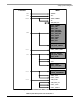

Setting up Power Management
i.MX53 System Development User’s Guide, Rev. 1
5-10 Freescale Semiconductor
5.3.2 I
2
C Acknowledge
The acknowledge signal is used for handshaking between the master and the slave. When the LTC3589-1
is written to, the LTC3589-1 acknowledges its write address and subsequent register address and data
bytes. When the LTC3589-1 is read from, it acknowledges its read address and 8-bit status byte.
An acknowledge pulse (active low) generated by the LTC3589-1 lets the master know that the latest byte
of information was transferred. The master generates the clock cycle and releases the SDA line (high)
during the acknowledge clock cycle. The LTC3589-1 pulls down the SDA line during the write
acknowledge clock pulse so that it is a stable Low during the high period of this clock pulse.
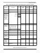
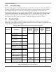
5.4 Interface Table
Table 5-2 shows the i.MX53 voltage rails, their power requirements, and their associated LTC3589-1
regulator in a typical application. Please note that system needs may vary according to the application, and
voltage rails must be adjusted accordingly.
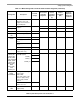
Table 5-2. i.MX53 Voltage Rails and Associated LTC3589-1 Regulator
Voltage Rail Description
Nominal
Voltage
Associated
LTC3589-1
Regulator
Voltage Set
Point of
LTC3589-1
Regulator
(V)
Current
Capability
(mA)
Power up
Sequence
Set at the
LTC3589-1
VDDGP ARM core supply voltage
fARM ≤ 400 MHz
0.95 SW1 1.1 1600 3
ARM core supply voltage
fARM 800 MHz
1.1
ARM core supply voltage
fARM 1000 MHz
1.25
ARM core supply voltage
Stop mode
0.85
VCC Peripheral supply voltage 1.3 SW2 1.3 1200 1
Peripheral supply voltage
Stop mode
0.95
VDDA Memory arrays voltage 1.3 LDO2 1.3 250 3
Memory arrays voltage -
Stop Mode
0.95
VDDAL1 L1 cable memory arrays
voltage
1.3 LDO2 1.3 250 3
L1 cable memory arrays
voltage—stop mode
0.95
VDD_DIG_PLL PLL Digital supplies
External regulator option
1.3 Internal
regulator
1.3 125 2
VDD_ANA_PLL PLL Analog supplies
External regulator option
1.8 Internal
regulator
1.8 125 2