
User`s guide


Setting up Power Management
i.MX53 System Development User’s Guide, Rev. 1
Freescale Semiconductor 5-9
5.3 Interfacing the i.MX53 Processor with LTC3589-1
The LTC3589-1 has flexible options for enabling and sequencing the regulator enables. The regulators are
enabled using input pins or the I
2
C serial port. To define a power-on sequence, tie the enable of the first
regulator to be powered up to the wake pin. Connect the first regulator’s output to the enable pin of the
second regulator, and so on. One or more regulators may be started in any sequence. Each enable pin has
a 200 μ (typical) delay between the pin and the internal enable of the regulator.
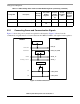
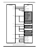
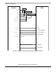
Figure 5-6 shows the power-up sequence for connecting the i.MX53 and the LTC3589-1 together as shown
in this chapter, taking into account the required extra regulators (TPS73201 and LT3481). The TPS7320’s
EN pin controls its output voltage, and the LT3481’s RUN/SS pin turns it on. Voltage sources are divided
into four different sets, according to the time they turn on.
Figure 5-6. Power-up Sequence
5.3.1 Using the I
2
C Interface
The LTC3589-1 uses the standard I
2
C 2-wire interface for communication with bus masters. The two bus
lines, SDA and SCL, must be high when the bus is not in use. External pull-up resistors or current sources
are required on these lines.
The LTC3589-1 is both a slave receiver and slave transmitter. The I
2
C control signals, SDA and SCL, are
scaled internally to the DVDD supply. DVDD should be connected to the same power supply as the bus
pull-up resistors.
The I
2
C port has an under voltage lockout on the DVDD pin. When DVDD is below approximately 1 V,
the I
2
C serial port is reset to power-on states and registers are set to default values.
Note: i.MX53 internal regulators are turned on at this point
LDO1
SW2
SW3
(Note 1)
SET 1 SET 2 SET 3 SET 4 SET 5
SW1
LDO2
LT3481
SW4
LDO3