
User`s guide


Setting up Power Management
i.MX53 System Development User’s Guide, Rev. 1
5-4 Freescale Semiconductor
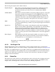
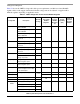
Table 5-1 shows the i.MX53 voltage rails, their power requirements, and their associated DA9053
regulator. Most of the supply domains have flexible voltage and can be adjusted or supplied with a
different regulator depending on application needs.
Table 5-1. i.MX53 Voltage Rails and Associated DA9053 Regulator
Voltage Rail Description
Nominal
Voltage
Associated
DA9053
Regulator
Voltag e S et
Point of
DA9053
Regulator
(V)
Current
Capability
(mA)
Power up
Sequence
Set at the
DA9053
VDDGP ARM core supply voltage
fARM ≤ 400 MHz
0.95 VBUCKCORE 1.1 2000 3
ARM core supply voltage
fARM ≤ 800 MHz
1.1
ARM core supply voltage
fARM ≤ 1000 MHz
1.25
ARM core supply voltage
Stop mode
0.85
VCC Peripheral supply voltage 1.3 VBUCKPRO 1.3 1000 1
Peripheral supply voltage—
stop mode
0.95
VDDA Memory arrays voltage 1.3 LDO10 1.3 250 2
Memory arrays voltage—
stop mode
0.95
VDDAL1 L1 cable memory arrays voltage 1.3 LDO6 1.3 150 2
L1 cable memory arrays
voltage—stop mode
0.95
VDD_DIG_PLL PLL digital supplies
External regulator option
1.3 LDO2 1.3 100 4
VDD_ANA_PLL PLL analog supplies
External regulator option
1.8 LDO8 1.8 200 2
NVCC_CKIH ESD protection of the CKIH pins,
Fuse read supply and 1.8 V bias
for the UHVIO pads
1.8 LDO8 1.8 200 2
NVCC_LCD GPIO digital power supplies 1.8 or
2.775
LDO4 2.775 150 5
NVCC_JTAG LDO8 1.8 200 2
NVCC_LVDS LVDS interface supply 2.5 VBUCKPERI_
SW
2.475 1000 4
NVCC_LVDS_BG LVDS band gap supply 2.5
NVCC_EMI_
DRAM
DDR supply DDR2 range 1.8 VBUCKMEM 1.5 1000 4
DDR supply LP-DDR2 range 1.2
DDR supply LV-DDR2 range 1.55
DDR supply DDR3 range 1.5