White Paper Implementing MLC NAND Flash for Cost-Effective, High-Capacity Memory Written by: Raz Dan and Rochelle Singer JANUARY 2003 91-SR-014-02-8L, REV 1.
Implementing MLC NAND Flash for Cost-Effective, High-Capacity Memory Introduction Multi-Level Cell (MLC) technology greatly reduces flash die size to achieve a breakthrough cost structure. It does this by storing 2 bits of data per physical cell instead of the traditional 1 bit per cell, using Binary flash technology. But the increased density of the MLC flash media has grave consequences in terms of data reliability and performance.
Implementing MLC NAND Flash for Cost-Effective, High-Capacity Memory of NOR flash and achieving barely adequate reliability, but it has serious limitations: its performance is far slower than standard NOR flash. NAND flash appeared to be the ideal media for data storage, due to its high-speed erase and write, high density (thus high capacity) and small size, as compared with NOR and AND devices.
Implementing MLC NAND Flash for Cost-Effective, High-Capacity Memory Select Gate Program (Inject electrons) Oxide Floating Gate eSource Erase (Remove electrons) Drain Substrate Figure 1: A Basic Flash Cell Binary and MLC Technologies In flash devices that implement Binary flash technology, there are two possible ranges for VTh. MLC technology can have several valid ranges for VTh, instead of just two. The first implementation of MLC uses four voltage levels (see Figure 2).
Implementing MLC NAND Flash for Cost-Effective, High-Capacity Memory MLC Benefits and Limitations MLC high-density design innovations reduce the silicon die size, which is the major element contributing to overall device cost. For MLC NAND, this reduction in size and cost is greatest in capacities of 256Mbit (32MByte) and higher, where the die can be as small as 50 percent of the size required to provide the same capacity Binary flash device.
Implementing MLC NAND Flash for Cost-Effective, High-Capacity Memory Read Disturb Errors The read disturb effect causes a page read operation to induce a permanent, bit value change in one of the read bits. In Binary flash technology based on a 0.16µ manufacturing process, the typical read disturb error rate is on the order of 1 bit error per 106 repetitive reads of the page containing the bit.
Implementing MLC NAND Flash for Cost-Effective, High-Capacity Memory Sustained Read When comparing sustained read performance values in real-world scenarios for Binary Flash with MLC, the gap lessens considerably: MLC performance is 98 percent of Binary flash performance.
Implementing MLC NAND Flash for Cost-Effective, High-Capacity Memory Overcoming MLC Limitations Because MLC technology can potentially bring the industry breakthrough cost and size benefits for local data and code storage, M-Systems chose to take on the challenge of perfecting it by providing solutions to overcome MLC reliability, performance and flash management limitations.
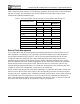
Implementing MLC NAND Flash for Cost-Effective, High-Capacity Memory Table 1 maps the various features of x2 technology against the three major areas of MLC limitations that they overcome. The remainder of this section explains how each feature achieves these enhancements in Mobile DiskOnChip G3.
Implementing MLC NAND Flash for Cost-Effective, High-Capacity Memory Enhanced EDC and ECC The Error Detection Code (EDC) and Error Correction Code (ECC) developed for x2 technology is based on M-Systems’ highly effective combination used in previous generation DiskOnChip products. This system contains hardware-embedded EDC mechanism to detect errors on-the-fly and software-embedded ECC mechanism to reduce silicon size and cost.
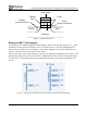
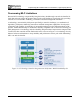
Implementing MLC NAND Flash for Cost-Effective, High-Capacity Memory Efficient Bad Block Handling x2 technology handles bad blocks, which can be randomly present in flash media, by enabling unaligned block access to two planes. Bad blocks are mapped individually on each plane, as shown in Figure 4. Good units can therefore be aligned or unaligned, minimizing the effects of bad blocks on the media.
Implementing MLC NAND Flash for Cost-Effective, High-Capacity Memory MultiBurst To improve MLC read performance rates, x2 technology incorporates a feature called MultiBurst. MultiBurst enables parallel read access from two 16-bit planes to the flash controller, thereby achieving the desired output data rate for the host. The host accesses the first word of a page with a relatively slow access time, but each subsequent word with a very fast access time.
Implementing MLC NAND Flash for Cost-Effective, High-Capacity Memory Parallel Multiplane Access As discussed earlier, the MLC flash media is built of two planes that can operate in parallel. This architecture is one of the most powerful, x2 technology innovations, doubling read, write and erase performance. Two pages on different planes can be concurrently read or written if they have the same offset within their respective blocks, even if the blocks are unaligned.
Implementing MLC NAND Flash for Cost-Effective, High-Capacity Memory How to Contact Us Website: http://www.m-sys.com General Information: info@m-sys.com Technical Information: techsupport@m-sys.com USA China M-Systems Inc. 8371 Central Ave, Suite A Newark CA 94560 Phone: +1-510-494-2090 Fax: +1-510-494-5545 M-Systems China Ltd. 25A International Business Commercial Bldg. Nanhu Rd., Lou Hu District Shenzhen, China 518001 Phone: +86-755-2519-4732 Fax: +86-755-2519-4729 Taiwan M-Systems Asia Ltd.