
Datasheet
LUXEON LED Assembly and Handling Application Brief AB32 20121217 9
2. Board Design Rules
2.1 PCB Requirements
A LUXEON LED is designed to be mounted on a two-layer FR4 PCB (Printed Circuit Board), a multi-layer FR4 PCB or an MCPCB (Metal Core
Printed Circuit Board). To ensure optimal operation of a LUXEON LED, the thermal path between the LED package and the heat sink should have a
thermal resistance as low as feasible.
Historically, MCPCB has been used for its low thermal resistance and rigidity. However, MCPCB is not always the most economical solution for
certain applications. A two layer FR4 board (with open vias or filled and capped vias), in contrast, often offers a much lower cost solution for a
thermally efficient package. By following the guidelines outlined below, one can achieve a thermal resistance for FR4 PCB that is equivalent to or
lower than a MCPCB equivalent design with lower cost than that of MCPCB.
For reference, here are the applicable IPC standards when designing PCB boards.
- General PCB design:
• IPC A-610D: Acceptability of Electronic Assemblies
- Filled and capped via boards:
• IPC 4761: Design Guide for Protection of Printed Board Via Structures
• IPC 2315: Design Guide for High Density Interconnects and Micro Vias
• IPC 2226: Design Standard for High Density Interconnect Printed Boards
2.2 LUXEON LED Footprint and Land Pattern
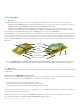
Philips Lumileds has conducted an investigation to determine the optimal land pattern design for a LUXEON LED on a PCB. The goal of this study
was to create a board with low thermal resistance, high placement accuracy, a minimum number of solder voids, and solderability indicators.
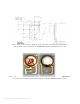
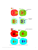
Figure 8 shows the individual layers of the suggested layout with solderability indicators for an open via Plated Through Hole (PTH) board design.
The green solder mask is a photolithographic mask, which offers a highly accurate alignment to the copper layer. The white mask labeled “White
Text” is a printed layer consisting of a double printed layers of for instance, Tamura USI - 210WP ink (UL E38152). This white layer enhances light
reflectivity, but is optional.
The solderability indicators, shown as the diagonally extended copper areas on the thermal and electrical land patterns, provide visual proof of
effective solder reflow on all pads. In addition to acting as solderability indicators, the extended area can also be electrically probed during quality
control tests. Reflow placement accuracy and thermal resistance will not be affected by the removal of the solderability indicators in the layout.
In this discussion, the term Land Pattern refers to the pattern on the PCB for the pads of a LUXEON LED.
The land pattern designs are available as .dxf file on the Philips Lumileds website at www.philipslumileds.com.