
Datasheet

LUXEON LED Assembly and Handling Application Brief AB32 20121217 24
5. Assembly Process Recommendations and Parameters
5.1 Stencil Design
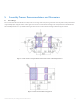
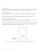
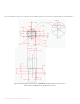
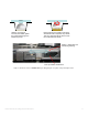
The recommended solder stencil thickness is 125µm. The area coverage of the solder paste is greater than 90%. This yields a solder joint thickness
of approximately 50µm, using the lead-free solder. Figure 31 shows the recommended stencil design for the footprint with two small thermal vias
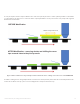
and solderability indicators for open via PTH board. Figure 32 shows the recommended stencil design for filled and capped via board.
Figure 31. Solder stencil for footprint with two thermal vias and four solder ability indicators.
Figure 32. Solder stencil for filled and capped via.