
Datasheet

LUXEON LED Assembly and Handling Application Brief AB32 20121217 19
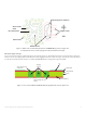
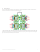
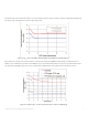
For filled and capped via, a low thermal resistance can be achieved with a minimum component spacing of 0.3mm for a 35µm/70µm (through-hole/
total surface) copper plating thickness as shown in Figure 23 (blue line).
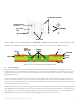
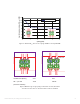
Figure 24 shows a comparison of the thermal resistance of various board technologies. MCPCB uses 35µm plating, open PTH via board uses
70/35µm copper and filled and capped via board uses 85/35µm copper. Note that the default number of vias is 33 for open PTH and 27 for filled
and capped via for 8mm LED spacing. Fewer vias are employed when the LED spacing is reduced which increases the thermal resistance.
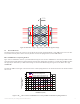
Figure 23. Rθ
c-hs
values of the PCB for different LED spacing and different via plating thicknesses.
Figure 24. Comparison Rθ
c-hs
of various board technologies as a function of LED spacing.