
Datasheet
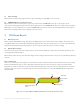

LUXEON LED Assembly and Handling Application Brief AB32 20121217 16
3.5 Thermal Resistance
The thermal resistance between the component case (body) and the back of the board/heatsink (Rθ
c-hs
) of the PCB depends on the size of Cu
area around the thermal pad, the number of vias, the placement of vias, the Cu plating thicknesses, and the PCB thickness.
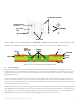
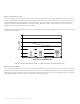
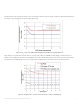
Effect of PCB thickness and plating thickness
Figure 19 shows simulated Rθ
c-hs
values for open PTH and filled and capped via as a function of PCB thickness. A double layer FR4 board with
various through hole plating thicknesses (20µm and 35µm) and total surface plating (50µm and 70µm for open PTH, 70µm and 85µm for filled
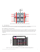
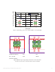
and capped via) are studied. The open PTH via board design uses 33 vias and the filled and capped design uses 27 vias. Data is for a single
LUXEON LED.
The thicker the PCB board, the higher is the thermal resistance. Thicker plating thickness for the thermal via will reduce the thermal resistance
and vice versa.
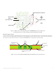
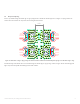
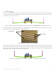
Figure 18. Illustration of edge to edge spacing for a filled and capped via design.
0
2
4
6
8
10
12
14
16
0.50.6 0.70.8 0.91 1.11.2 1.31.4 1.51.6 1.7
PCB thickness (mm)
board thermal resistance
Rth
c-hs
(K/W)
Open via PTH Cu plating 70 / 35
Open via PTH Cu plating 50/ 20
filled and capped via Cu plating 85 / 35
filled and capped via Cu plating 70 / 20
Figure 19. Rθ
c-hs
values as function of PCB thickness for two layers FR4 board with different plating thicknesses.
0.30