
Datasheet

LUXEON LED Assembly and Handling Application Brief AB32 20121217 13
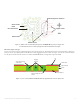
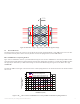
A multilayer FR4 board with filled and capped via may be considered. See Figure 14 for a cross section of the multilayer board design.
3.3 Thermal Via Design
For both the open via PTH and filled and capped via design, the finished hole diameter is 0.5mm. A smaller diameter will lead to an increased
thermal resistance. The recommended distance between two holes is 0.4 mm. This results in a minimal pitch of 0.9 mm between the vias. Figure
15 indicates the typical dimensions. The position of the vias may differ from the preferred layout of Figure 11 and Figure 13, without significantly
changing thermal properties.
For open via PTH design, the drill hole for the two smaller vias with a 35µm plating thickness is 0.32mm. The solder mask area around the vias is
needed to avoid solder to flow through the vias to the backside. This would lead to a reduced heat sink contact of the PCB bottom surface. An
opening in the solder mask of 0.05mm surrounds each via. The total minimal width of the solder mask around the via is 0.25 mm. Figure 16 shows
the resulting solder mask design of the thermal pad.
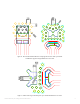
For filled and capped via design, each via is filled or plugged with an epoxy material. Standard industry practices recommend using a plugging material
with a CTE (Coefficient of Thermal Expansion) and Tg to match the thermal characteristics of the PCB. Recommendations on qualification criteria
for the plugging process are documented in IPC-4761 “Design Guide for Protection of Printed Board Via Structures”. Use of thermally improved
plugging material can further reduce the board thermal resistance, although the absolute improvement will be small.
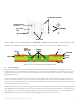
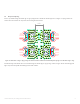
Figure 13. Outline of the recommended pad layout for a LUXEON LED on a PCB with filled and capped vias. See Figure 9 for alternate views.
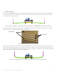
Figure 14. Cross section of filled and capped via multilayer board.
Copper traces
Etched copper for isolation
Filled and capped
thermal via
Green solder
mask
White text
Solder stencil
Copper traces Copper traces
Etched copper for isolation
Filled and capped
thermal via
Green solder
mask
White text
Solder stencil
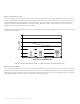
Ink
Copper
Solder Mask
Epoxy
Plugging
material
Copper
plating on top
of filled vias
Copper
Copper
Laser via
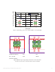
Ink
Copper
Solder Mask
Epoxy
Plugging
material
Plugging
material
Copper
plating on top
of filled vias
Copper
Copper
Laser via