
Datasheet

LUXEON LED Assembly and Handling Application Brief AB32 20121217 12
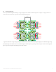
Filled and capped via design
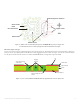
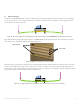
A cross section of this design for a standard two layers board is shown in Figure 12. The final thermal resistance is determined by the number and
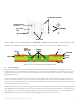
density of vias, the copper plating thickness, PTH thickness and the plugging material used to fill the vias. Figure 13 shows the recommended layout
for a two layer board. The thermal resistance for a 0.8mm thick FR4 PCB with these design features approaches 3K/W.
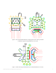
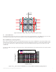
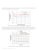
Figure 11. Outline of the recommended pad layout for a LUXEON LED (top view). See Figure 8 for
more illustrations. There is 0.5mm spacing between the thermal and electrical pads.
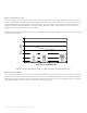
Ink
Copper (85µm)
Solder Mask
Epoxy
Plated through hole via
(
35
µ
m
)
Plugging
material
25um plang on top
of filled vias
Copper (85µm)
Figure 12. Cross section of FR4 based PCB with filled and capped thermal via for two layer board.
13
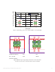
Green solder
mask
PTH Thermal via
White text
Copper traces
Solder stencil
Etched copper for isolation