
Datasheet

LUXEON LED Assembly and Handling Application Brief AB32 20121217 11
2.3 Surface Finishing
Philips Lumileds recommends using a high temperature organic solderability preservative (OSP) on the copper layer.
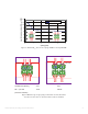
2.4 LUXEON LED Close Proximity Placement
Philips Lumileds recommends a minimal edge to edge spacing of 0.3mm between LUXEON LEDs. If the edge to edge spacing is less, the
components may drift together during the solder step. Also, the light output for each LUXEON LED may drop due to optical absorption by adjacent
LED packages. For open via PTH design, close spacing of LUXEON LEDs may require the removal of the solderability indicators shown in Figure 8.
Removal of the solderability indicators does not affect the placement accuracy.
3. FR4-Based Boards
3.1 Material Properties
FR4 is an industry standard PCB technology. Depending on the LED application, drive condition and the number of LEDs on the board, the choice
for Tg (Glass Transition Temperature) and CTI (Comparative Tracking Index) value of the base material needs to be set. Most common FR4 material
has Tg=130°C and CTI=175V. For high voltage applications, the trace clearances and CTI values may be increased accordingly.
3.2 Optimal Thermal Design
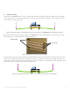
Thermal vias are the primary method of heat transportation to the heat sink at the PCB bottom. A thermal via is a plated through hole that can be
open, plugged, filled or filled and capped.
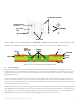
Philips Lumileds conducted a study on two thermal via designs aimed at reducing the thermal resistance. They are (a) open via PTH and (b) filled and
capped via.
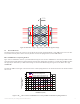
Open via PTH design
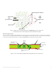
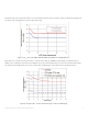
A cross section of this design is shown in Figure 10. The final thermal resistance is determined by the number and density of vias, the copper plating
thickness and PTH thickness. Figure 11 shows a design with a standard two layer board. Here the total copper plating is 70µm with the PTH
plating thickness of 35um. In total, 33 vias are placed outside the thermal landing pad. The placement of the two smaller thermal vias is to minimize
voiding in the solder joint. For the recommended design, the measured thermal resistance for a 0.8mm thick FR4 PCB with these design features
approaches 7K/W.
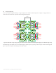
Ink
Copper (70µm)
Solder Mask
Epoxy
Plated through hole via
(
35
µ
m
)
Copper (70µm)
Figure 10. Cross section of FR4 based PCB with thermal vias to decrease the thermal resistance.