LUXEON LED Assembly and Handling Information Application Brief AB32 LUXEON® LED Assembly and Handling Information For LUXEON Rebel, LUXEON Rebel ES, LUXEON A, and LUXEON R LEDs Introduction This application brief covers recommended board designs and assembly procedures for the LUXEON LEDs referenced above. LUXEON LEDs are revolutionary, ultra-compact, surface mount, high-power LEDs. These LEDs offer a compact package with high lumen output and superior thermal performance.
Scope The assembly and handling guidelines in this Application Brief apply to the following LUXEON products: - LUXEON Rebel - LUXEON Rebel Color - LUXEON Rebel Automotive - LUXEON Rebel ES - LUXEON A - LUXEON R The LEDs that belong to these product categories have very similar form factors. Consequently, most handling requirements and board design recommendations in this Application Brief apply to all LEDs. Any handling requirements that are specific to a subset of LUXEON LEDs will be clearly marked.
Table of Contents 1. Component................................................................................................................................................................. 4 1.1. Description......................................................................................................................................................... 4 1.2. Optical Center..............................................................................................................................
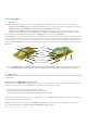
1. Component 1.1. Description A LUXEON LED is a revolutionary, ultra-compact, surface mount, high-power LED which comes in two different mechanical configurations: - Configuration A: A LUXEON LED with this configuration has a flat surface area outside the silicone lens. This configuration is used for all LUXEON Rebel Color and LUXEON Rebel White LEDS (datasheets DS58, DS63, DS64, and DS68).
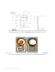
Figure 2. The most accurate method to find the theoretical optical center and the center of the silicone lens is by using the fiducials located on the front side of a LUXEON LED (configuration A). All dimensions are in mm. Figure 3. Top views of AlInGaP and InGaN LUXEON LEDs (configuration A). The fiducials on an AlInGaP LUXEON LED (left) are connected to the metallization patterns while the fiducials on an InGaN LUXEON LED (right) are isolated.
Fiducial Marks for a LUXEON LED (configuration B): A LUXEON LED (configuration B) has two fiducial marks labeled F1 and F2 as shown in Figure 4. An optional third fiducial, F3, may be present as well. These fiducial marks provide the most accurate methodology to locate the theoretical optical center, marked by the red dot in Figure 4. The theoretical optical center is located 1.450mm from the vertical and horizontal edges of fiducial marks F1 and F2. The theoretical optical center also lies 1.
LED Outline and Backside Metallization While the fiducial marks provide the most accurate technique to find the optical center of the silicone lens, one can also use the edges or the backside metallization to locate the theoretical optical center of a LUXEON LED. Figure 2 and Figure 4 illustrate the position of the optical center with respect to the edges of the ceramic substrate for the two different LUXEON LED configurations. In both configurations the optical center is located 1.
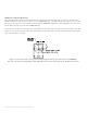
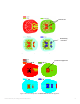
1.3 Lens Handling A LUXEON LED is designed to maximize light output and reliability. However, improper handling of a LUXEON LED may damage the silicone lens and affect the overall light performance and reliability. To minimize the risk of damage to the silicone lens during manual handling, only pick up LUXEON LEDs from the sides of the ceramic substrate and never from the silicone lens itself (see Figure 7). Figure 7. Correct handling (left) and incorrect handling (right) of a LUXEON LED.
2. Board Design Rules 2.1 PCB Requirements A LUXEON LED is designed to be mounted on a two-layer FR4 PCB (Printed Circuit Board), a multi-layer FR4 PCB or an MCPCB (Metal Core Printed Circuit Board). To ensure optimal operation of a LUXEON LED, the thermal path between the LED package and the heat sink should have a thermal resistance as low as feasible. Historically, MCPCB has been used for its low thermal resistance and rigidity.
Thermal vias Solderability indicators Figure 8. Recommended layout for a LUXEON LED with open via PTH board. Filled and capped via Figure 9. Recommended layout for a LUXEON LED with filled and capped vias.
2.3 Surface Finishing Philips Lumileds recommends using a high temperature organic solderability preservative (OSP) on the copper layer. 2.4 LUXEON LED Close Proximity Placement Philips Lumileds recommends a minimal edge to edge spacing of 0.3mm between LUXEON LEDs. If the edge to edge spacing is less, the components may drift together during the solder step. Also, the light output for each LUXEON LED may drop due to optical absorption by adjacent LED packages.
Etched copper for isolation Green solder mask Copper traces PTH Thermal via White text 13 Solder stencil Figure 11. Outline of the recommended pad layout for a LUXEON LED (top view). See Figure 8 for more illustrations. There is 0.5mm spacing between the thermal and electrical pads. Filled and capped via design A cross section of this design for a standard two layers board is shown in Figure 12.
Etched copper for isolation Filled and capped thermal via Copper traces Green solder mask White text Solder stencil Figure 13. Outline of the recommended pad layout for a LUXEON LED on a PCB with filled and capped vias. See Figure 9 for alternate views. A multilayer FR4 board with filled and capped via may be considered. See Figure 14 for a cross section of the multilayer board design.
Figure 15. Recommended finished diameter and spacing dimensions for both open via PTH and filled and capped via design. All dimensions are in mm. Figure 16. Solder mask design of thermal pad for open via PTH. All dimensions are in mm.
3.4 Component Spacing For the open via PTH design, the minimal edge to edge spacing is 4mm to maintain the thermal properties, see Figure 17. Spacing below 4 mm results in fewer vias between the components, thus increasing thermal resistance. 4.00 Figure 17. Illustration of edge to edge spacing. The thermal resistance will increase dramatically if the spacing is less than 4mm edge to edge. For filled and capped vias with the above recommended design, the minimal edge to edge spacing is 0.
0.30 Figure 18. Illustration of edge to edge spacing for a filled and capped via design. 3.5 Thermal Resistance The thermal resistance between the component case (body) and the back of the board/heatsink (Rθc-hs) of the PCB depends on the size of Cu area around the thermal pad, the number of vias, the placement of vias, the Cu plating thicknesses, and the PCB thickness.
Impact of the thermal via count For an open via PTH board, removal of the 14 outer vias increases the thermal resistance by approximately 1K/W. The 14 outer vias are labeled in Figure 11. Eliminating the two smaller vias in the thermal landing pad increases the Rθc-hs value by 1 K/W as well since the copper area around the thermal landing pad has a large contribution to the thermal spreading. The optimal copper area extends 3mm beyond the thermal pad.
board thermal resistance Rth c-hs (K/W) 14 Rth (c-hs) 4LED cluster 12 10 8 6 4 2 0 0 1 2 3 4 5 spacing (mm) Figure 21. Simulated Rθc-hs values for close spacing of LEDs for a two layer FR4 PCB. 124 Vias 90 Vias LUXEON LED Spacing 2mm 4mm Rθc-hs per LED 7K/W 6.8K/W (simulation estimate) Figure 22. When the edge to edge spacing is reduced from 4 to 2mm, the number of vias decreases from 124 to 90. Thermal resistance values are simulated.
For filled and capped via, a low thermal resistance can be achieved with a minimum component spacing of 0.3mm for a 35µm/70µm (through-hole/ total surface) copper plating thickness as shown in Figure 23 (blue line). Figure 23. Rθc-hs values of the PCB for different LED spacing and different via plating thicknesses. Figure 24 shows a comparison of the thermal resistance of various board technologies.
3.6 FR4 Board Handling The substrate of a LUXEON LED is made of ceramic, a relatively brittle material. Even though this product has a small form factor and is unlikely to cause any problems, forces on the package should be kept to a minimum. In particular, excessive bending forces on the package may crack the ceramic substrate or break the solder joints. Figure 25. Excessive bending force on the PCB may crack the ceramic substrate of a LUXEON LED and/or damage the solder joints.
Board warpage can be minimized by understanding how different CTE materials are stacked up. For example, when an FR4 board is sandwiched between two full copper sheets, adding thin isolation lines in the copper sheet to create copper islands can minimize board warpage as shown in Figure 28. Copperisola on isolation Copper Figure 28. Copper islands can help reduce board warpage.
4. MCPCB Board design The layout for the MCPCB design is similar to the FR4 layout in Figure 8 but without all the vias, see Figure 29. Copper Solder Mask Epoxy White Ink Solder Figure 29. Recommended layout for a LUXEON LED on MCPCB. Note that this layout is similar to the FR4 layout in Figure 8 but without all the vias. In order to minimize thermal resistance the area of copper connected to the thermal pad of a LUXEON LED must be maximized.
Table 1 summarizes thermal resistance values for typical and high thermal conductivity epoxies. Standard MCPCB design rules yield a board with 10K/W thermal resistance. Increasing the copper thickness and using a thinner dielectric with higher thermal conductivity lowers the thermal resistance dramatically. In both cases the copper area extending outside the thermal pad is at least 3mm. Table 1.
5. Assembly Process Recommendations and Parameters 5.1 Stencil Design The recommended solder stencil thickness is 125µm. The area coverage of the solder paste is greater than 90%. This yields a solder joint thickness of approximately 50µm, using the lead-free solder. Figure 31 shows the recommended stencil design for the footprint with two small thermal vias and solderability indicators for open via PTH board. Figure 32 shows the recommended stencil design for filled and capped via board. Figure 31.
5.2 Solder Paste Philips Lumileds recommends lead-free solder for a LUXEON LED. Philips Lumileds successfully tested SAC 305 solder paste from Alpha Metals (OM338 grade 3 and OM 325 grade 4) with satisfactory results. However, since application environments vary widely, Philips Lumileds recommends that customers perform their own solder paste evaluation in order to ensure it is suitable for the targeted application. 5.
To prevent the LED from sticking to the nozzle after placement, Philips Lumileds uses the mold release spray SR3-500B from Solent Maintenance. Figure 34. Dedicated pick-up nozzle design for a LUXEON LED (configuration A). The nozzle tolerances must account for the LED dimensions. All dimensions are in mm.
Pick and place for LUXEON LEDs (configuration B) A Philips Lumileds specific nozzle can be used for pick and place of LUXEON LEDs (configuration B), see Figure 35. This nozzle picks up from the flat area around the silicone lens and does not make any contact with the silicone lens of a LUXEON LED. Figure 35. Dedicated pick-up nozzle design for a LUXEON LED (configuration B).
5.4 Pick and Place Machine Optimization Table 2 below summarizes key pick and place parameters for the dedicated LUXEON LED nozzles based on Philips Lumileds internal test results. Since pick and place settings vary between pick and place tools and vendors, Philips Lumileds recommends that these parameters are used as a reference only. Table 2. LUXEON LED (configuration A) LUXEON LED (configuration B) -1.
Shutter After the cover tape is removed, the shutter guides the component through the feeder for pick up. During indexing, the shutter moves back and forth and the component may vibrate. This may cause the silicone lens to come into contact with the shutter. Shutter – slides back and forth during indexing Pick up nozzle is located here Figure 37. The silicone lens of a LUXEON LED may be damaged by the cover plate of the pick and place feeder.
In some pick and place machines a simple modification can be made to the pick and place feeder to achieve optimum yield. One recommendation to reduce damage to the silicone lens is to remove the shutter completely and shift the cover tape removal close to the pick-up nozzle. Figure 38 illustrates this recommendation. BEFORE Modification Shutter moving back & forth AFTER Modification – removing shutter and shifting the cover tape removal close to the pick-up nozzle Figure 38.
5.5 Placement Accuracy In order to achieve the highest placement accuracy Philips Lumileds recommends using an automated pick and place tool with a vision system that can recognize the bottom metallization of a LUXEON LED (3 pads). If available use the SOT32 profile from the component library, and modify the lead dimensions and pitch according to the dimensions in Figure 39. The recognition tolerance can be set to 30%. A lower percentage improves placement accuracy but may reduce recognition yield.
5.6 Reflow Profile LUXEON LEDs are compatible with surface mount technology and lead-free reflow. This greatly simplifies the manufacturing process by eliminating the need for adhesives and epoxies. It has been said that the most important step in reflow soldering is the reflow itself. This occurs when the boards move through the oven and the solder paste melts forming the solder joints. To form good solder joints, the time and temperature profile throughout the reflow process must be well maintained.
5.7 Reflow Accuracy Global fiducials on the PCB board (see Figure 41) can help calculate the reflow accuracy between the centers of the component to the nominal board position. Section 1.2 Optical Center explains how to find the theoretical optical center of the LUXEON LED. Philips Lumileds has determined the placement accuracy after reflow to be well within 90µm in the x and y directions for the footprint of Figure 11.
5.8 Void Inspection and Solderability Indicators An in-line X-Ray machine can inspect for voids after reflow. Philips Lumileds has determined that the two small thermal vias in the thermal pad footprint minimizes voiding by serving as an air vent during reflow. A large percentage of voids in the thermal pad will increase of the thermal resistance. Figure 42 and Figure 43 show the impact of solder voiding on board thermal resistance (Rθc-hs) based on modeled data. Figure 42.
1 3 2 4 Figure 44. A LUXEON LED reflowed onto an FR4 PCB with four solderability indicators.
6. JEDEC Moisture Sensitivity Level LUXEON LEDs have a JEDEC moisture sensitivity level of 1. This is the highest level offered in the industry and highest level within the JEDEC standard. This provides the customer with ease of assembly. The customer no longer needs to be concerned about bake out times and floor life. No bake out time is required for a moisture sensitivity level of 1.
7. Product Packaging Considerations – Chemical Compatibility LUXEON LEDs contain a silicone overcoat and silicone lens to protect the LED chip and extract the maximum amount of light. As with most silicones used in LED optics, care must be taken to prevent any incompatible chemicals from directly or indirectly reacting with the silicone. The silicone overcoat in the LUXEON LED is gas permeable. Consequently, oxygen and volatile organic compound (VOC) gas molecules can diffuse into the silicone overcoat.
Table 4. List of commonly used chemicals that will damage the silicone lens of a LUXEON LED. Avoid using any of these chemicals in the housing that contains the LED package.
Company Information Philips Lumileds is a leading provider of LEDs for everyday lighting applications. The company’s records for light output, efficacy and thermal management are direct results of the ongoing commitment to advancing solid-state lighting technology and enabling lighting solutions that are more environmentally friendly, help reduce CO2 emissions and reduce the need for power plant expansion.