
User's Manual
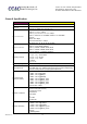
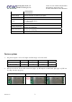
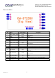
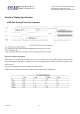
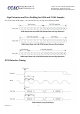
Table Of Contents

晶訊科技股份有限公司 8F, No. 150, Jian Yi Road, Zhonghe District,
CC&C Technologies, Inc. New Taipei City, Taiwan 235, R.O.C.
Tel: 886-2-8226-5088 Fax: 886-2-8226-5077
Version: 1.6
7
Pin outs define:
Pin Signal Input /Output Description
1 CHIP_WAKE_HOST Output
Signal from module to wake up host,refer driver source
code for details.
2 GND Power Ground
3 USB D+ I/O USB D+ signal
4 USB D- I/O USB D- signal
5 VCC Power DC 3.3V
6 HOST_WAKE_CHIP Input
Signal from host to wake up module,refer driver source
code for details.
7 GND Power Ground
8 ANT RF WLAN/BT RF port (if don’t using IPEX connector)
9 GND Power Ground
10 BT_PCM_IN Input
PCM data Input. This pin is also shared with GPIO0 and
3DG_SEL_A.
11 BT_PCM_OUT Output
PCM data Output. This pin is also shared with GPIO1 and
3DG_SYNC_A.
12 BT_PCM_SYNK I/O
PCM frame Synchronization. This pin is also shared with
GPIO2.
13 BT_PCM_CLK I/O PCM Clock. This pin is also shared with GPIO3.
14 EXT_XIN - NC_ Keep to floating