
User Manual

13
7.1.0 Component Choice and Placement
7.1.1 bitSnap connectors must not be moved from their original
positions in the templates.
7.1.2 All components besides bitSnap connectors which are
included in the templates may be moved and their traces
rerouted if necessary.
7.1.3 Resistors, capacitors, inductors, and other 2-lead passives
should be SMD0603 chip devices unless design
requirements do not allow it.
7.1.4 BGA packages are not allowed; QFNs are acceptable but
LB recommends SOICs as they are easier to work with.
IC packages should be as small as necessary, but no
smaller. Use good judgment, and consult littleBits with any
questions.
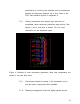
7.1.5 Pad spacing from component to component should be no
less than 0.024 inches (0.6096mm) unless design
requirements do not permit it. This spacing allows routing
of a minimum width 0.008-inch (0.2032mm) trace between
the pads without violating the minimum clearance
requirement.
7.1.6 Top layer components must be placed according to the
layout proposal found in the PRD.
7.1.7 Bottom layer components should be placed with electrical