
User Manual

12
7.0.4 Set the PCB layout primary grid to 0.1mm. Set the alternate grid
to 0.01mm.
7.0.5 The origin of the FRAME-LETTER package must be set to
coordinates (0, 0). All the other parts of the design must be
placed within the bounds of this frame.
7.0.6 The board outline and the dimension layer must not be altered.
7.0.7 All packages used must be from the LITTLEBITS140915.lbr littleBits
Eagle library. If specific device does not exist it must be created
and verified by littleBits.
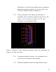
7.0.8 Minimum track width shall be 0.008 inches (0.2032mm). The
default width is 0.016 inches (0.4064mm). The default width
should generally be used when possible. There should also be a
1mm track from the VCC pin of the input bitSnap(s) to the VCC
pin of the output bitSnap(s) as exemplified in the templates.
7.0.9 Minimum clearance requirement shall be 0.008 inches (0.2032mm).
7.0.10 To assure that vias and polygons are rendered properly the Design
Rules File listed in the Preparations section (4.0.0) should be
loaded and an initial check run before the PCB is routed. If this is
not completed, EagleCAD will follow its default design rules and
can create problems later on in the design process.