
User Manual


10
does not exist it must be created and verified by littleBits.
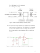
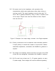
6.0.8 The circuit should read from left to right when possible.
6.0.9 Male bitSnap connectors are inputs, and must be placed on the
left side of the frame. Female bitSnap connectors are outputs, and
must be located on the right side of the frame.
6.0.10 The bitSnap symbol terminals are labeled VCC, SIG, and GND.
Each of these pins must be connected to the NET corresponding
to those labels.
6.0.11 Each Net connection should leave space to see the green Net line.
6.0.12 Every schematic symbol should have a reference designator in the
“NAME” field.
6.0.13 Every schematic symbol must have information in the “VALUE”
field. For passives, the value should be the component value (i.e.,
resistance in ohms, or capacitance in microFarads, etc.) and
semiconductors should list the manufacturer's part number (i.e.,
LV321 for our littleBits standard op amp).
6.0.14 “NAME” and “VALUE” fields must all be visible on the schematic.
The text should be legible and not overlap with other text or
symbols.
6.0.15 The Net GND must represent ground and the Net VCC must
represent Power.