
Datasheet


RoHS Compliant, ELV Compliant
262
11
Solder Reflow and Rework Recommendations for PolySwitch Telecommunications Surface-Mount
Devices
Solder Reflow
• Recommended reflow method: IR, vapor phase oven, hot air oven.
• Surface-mount devices are not intended to be wave soldered to the bottom side of the board.
• Recommended maximum paste thickness of 0.25mm (0.010in).
• Devices can be cleaned using standard industry methods and solvents.
Rework
• If a device is removed from the board, it should be discarded and replaced with a new device.
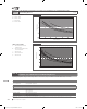
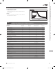
Profile Feature Pb-Free Assembly
Average ramp up rate (Ts
MAX
to Tp) 3°C/s max
Preheat
• Temperature min (Ts
MIN
) 150°C
• Temperature max (Ts
MAX
) 200°C
• Time (ts
MIN
to ts
MAX
) 60-180 s
Time maintained above:
• Temperature (T
L
) 217°C
• Time (t
L
) 60-150 s
Peak/Classification temperature (Tp) 260°C
Time within 5°C of actual peak temperature
Time (tp) 20-40 s
Ramp down rate 6°C/s max
Time 25°C to peak temperature 8min max
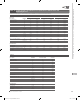
Critical Zone
T
L
to Tp
Ramp Up
t 25˚C to Peak
Reflow Profile
Time
Ramp Down
ts
Preheat
Ts
MAX
T
L
Tp
tp
25
Ts
MIN
t
L
Temperature
Figure T21
Note: All temperatures refer to topside of the package, measured on the package
body surface.
Agency Recognition for PolySwitch Telecommunications and Networking Devices
UL File # E74889
CSA File # 78165C
TÜV Per IEC60730-1 Certificate # for individual products available upon request.
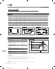
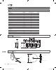
Device A B C D E F G Figure
TS250 (All) 4.60 1.80 6.10 — — — — T18
(0.180) (0.070) (0.240) — — — —
TSV250 (All) 2.29 2.41 6.35 3.43 — — — T19
(0.090) (0.095) (0.250) (0.135) — — —
TSL250 (All) 3.60 1.80 5.50 — — — — T18
(0.140) (0.070) (0.220) — — — —
TS600 (All) 10.42 3.30 3.35 — — — — T18
(0.410) (0.130) (0.132) — — — —
TSM600 (All) 5.20 17.80 5.54 6.75 2.08 3.12 8.39 T20
(0.205) (0.701) (0.218) (0.266) (0.082) (0.123) (0.331)
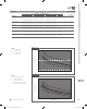
A
B CB
Figure T18
A
A
B B
C
D
Figure T19
A
B
C D
G
E
F
Figure T20
Table T7
Recommended Pad Layouts for Surface-mount PolySwitch Telecommunications and
Networking Devices in Millimeters (Inches) Nominal
2013_CP_S11-Poly-8-TeleNetwork.indd 262 8/3/13 10:41 AM