
User guide

© 2013 Littelfuse, Inc.
Specifications are subject to change without notice.
Revised: 11/25/13
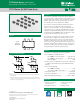
TVS Diode Arrays (SPA
®
Diodes)
General Purpose ESD Protection - SP724 Series
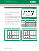
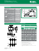
Package Dimensions — Small Outline Transistor Plastic Packages (SOT23-6)
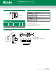
Time
Temperature
T
P
T
L
T
S(max)
T
S(min)
25
t
P
t
L
t
S
time to peak temperature
Preheat
P
rehea
t
Ramp-up
R
amp-up
Ramp-down
R
amp-d
o
Critical Zone
T
L to TP
C
ritical Zon
e
T
L
to
T
P
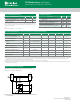
Reflow Condition Pb–Freeassembly
Pre Heat
- Temperature Min (T
s(min)
) 150°C
- Temperature Max (T
s(max)
) 200°C
- Time (min to max) (t
s
) 60–180secs
Average ramp up rate (Liquidus) Temp
(T
L
) to peak
5°C/secondmax
T
S(max)
to T
L
- Ramp-up Rate 5°C/secondmax
Reflow
- Temperature (T
L
) (Liquidus) 217°C
- Temperature (t
L
) 60–150seconds
Peak Temperature (T
P
) 260
+0/-5
°C
Time within 5°C of actual peak
Temperature (t
p
)
20–40seconds
Ramp-down Rate 5°C/secondmax
Time 25°C to peak Temperature (T
P
) 8minutesMax.
Do not exceed 260°C
Soldering Parameters
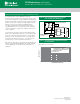
Notes:
1. DimensioningandtolerancesperANSI14.5M-1982.
2. PackageconformstoEIAJSC-74(1992).
3. DimensionsDandE1areexclusiveofmoldash,protrusions,orgateburrs.
4. FootlenthLmeasuredatreferencetoseatingplane.
5. “L”isthelengthofatfootsurfaceforsolderingtosubstrate.
6. “N”isthenumberofterminalpositions.
7. Controlingdimension:MILLIMETER.Convertedinchdimensionsarenotnecessarily
exact.
Package SOT23-6
Pins 6
JEDEC MO-178
Millimeters Inches
Notes
Min Max Min Max
A 0.900 1.450 0.035 0.057 -
A1 0.000 0.150 0.000 0.006 -
A2 0.900 1.300 0.035 0.051 -
b 0.350 0.500 0.0138 0.0196 -
C 0.080 0.220 0.0031 0.009 -
D 2.800 3.000 0.11 0.118 3
E 2.600 3.000 0.102 0.118 -
E1 1.500 1.750 0.06 0.069 3
e 0.95Ref 0.0374ref -
e1 1.9Ref 0.0748Ref -
L 0.100 0.600 0.004 0.023 4,5
N 6 6 6
a 0º 10º 0º 10º -
M 2.590 0.102 -
O 0.690 .027TYP -
P 0.990 .039TYP -
R 0.950 0.038 -
O
P
R
M
Recommended Solder Pad Layout