
User guide

© 2013 Littelfuse, Inc.
Specifications are subject to change without notice.
Revised: 11/25/13
TVS Diode Arrays (SPA
®
Diodes)
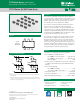
General Purpose ESD Protection - SP724 Series
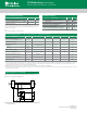
Absolute Maximum Ratings
Parameter Rating Units
ContinuousSupplyVoltage,(V+)-(V-) +20 V
ForwardPeakCurrent,I
IN
toV
CC
,GND
(RefertoFigure5)
±2.2,100µs A
Electrical Characteristics T
A
= -40
o
C to 105
o
C, V
IN
= 0.5V
CC
, Unless Otherwise Specified
Thermal Information
Parameter Rating Units
ThermalResistance(Typical,Note3) θ
JA
o
C/W
SOTPackage 220
o
C/W
MaximumStorageTemperatureRange -65to150
o
C
MaximumJunctionTemperature 150
o
C
MaximumLeadTemperature
(Soldering20-40s)(SOT-LeadTipsOnly)
260
o
C
CAUTION: Stresses above those listed in “Absolute Maximum Ratings” may cause
permanent damage to the device. This is a stress only rating and operation of the device
at these or any other conditions above those indicated in the operational sections of this
specification is not implied.
Note:3.θ
JA
ismeasuredwiththecomponentmountedonanevaluationPCboardinfreeair.
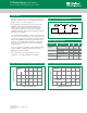
Parameter Symbol Test Conditions Min Typ Max Units
OperatingVoltageRange,
V
SUPPLY
=[(V+)-(V-)](Notes4,5)
V
SUPPLY
1 - 20 V
ForwardVoltageDrop
ForwardVoltageDrop
INtoV- V
FWDL
I
IN
=1A(PeakPulse) - 2 - V
INtoV+ V
FWDH
- 2 - V
InputLeakageCurrent I
IN
-10 1 10 nA
QuiescentSupplyCurrent I
QUIESCENT
V+=20V,V-=GND - - 100 nA
EquivalentSCRONThreshold (Note6) - 1. 1 - V
EquivalentSCRONResistance V
FWD
/I
FWD
(Note6) - 1. 0 - Ω
InputCapacitance C
IN
- 3 - pF
Notes:
4.Inautomotiveandotherbatterychargingsystems,theSP724powersupplylinesshouldbeexternallyprotectedforloaddumpandreversebattery.WhentheV+andV-Pinsareconnected
tothesamesupplyvoltagesourceasthedeviceorcontrollineunderprotection,acurrentlimitingresistorshouldbeconnectedinseriesbetweentheexternalsupplyandtheSP724
supplypinstolimitreversebatterycurrenttowithintheratedmaximumlimits.
5.Bypasscapacitorsoftypically0.01µForlargershouldbeconnectedcloselybetweentheV+andV-Pinsforallapplications.
6.RefertotheFigure3graphfordenitionsofequivalent“SCRONThreshold”and“SCRONResistance”.Thesecharacteristicsaregivenhereforinformationtodeterminepeakcurrentand
dissipationunderEOSconditions.
Note:
ESDRatingsandCapability-SeeFigure1,Table1
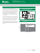
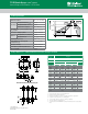
Typical Application of the SP724
+V
CC
INPUT
DRIVERS
SP724 INPUT PROTECTION CIRCUIT (1 OF 4 SHOWN)
OR
SIGNAL
SOURCES
IN 1, 3, 4 AND 6
SP724
V-
TO +V
CC
LINEAR OR
DIGITAL IC
INTERFAC E
V+
+V
CC
0.001µF
FIGURE 4. TYPICAL APPLICATION OF THE SP724 AS AN INPUT CLAMP FOR OVER-VOLTA GE, GREATER THAN 1V
BE
ABOVE V+ OR
LESS THAN -1V
BE
BELOW V-
ApplicationasanInputClampforOver-voltage,Greaterthan1V
BE
AboveV+orlessthan-1V
BE
belowV-)