
Manual

© 2013 Littelfuse, Inc.
Specifications are subject to change without notice.
Revised: 04/24/13
TVS Diode Arrays (SPA
®
Diodes)
General Purpose ESD Protection - SP723 Series
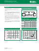
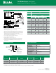
Absolute Maximum Ratings
Parameter Rating Units
Continuous Supply Voltage, (V+) - (V-) +35 V
Forward Peak Current, I
IN
to V
CC
, I
IN
to
GND (Refer to Figure 5)
±4, 100µs A
Peak Pulse Current, 8/20µs ±7 A
Electrical Characteristics T
A
= -40
o
C to 105
o
C, V
IN
= 0.5V
CC
, Unless Otherwise Specified
Thermal Information
Parameter Rating Units
Thermal Resistance (Typical, Note 1) θ
JA
o
C/W
PDIP Package 160
o
C/W
SOIC Package 170
o
C/W
Storage Temperature Range -65 to 150
o
C
Maximum Junction Temperature (Plastic
Package)
150
o
C
Lead Temperature
(Soldering 20-40s) (SOIC Lead Tips Only)
260
o
C
CAUTION: Stresses above those listed in “Absolute Maximum Ratings” may cause
permanent damage to the device. This is a stress only rating and operation of the device
at these or any other conditions above those indicated in the operational sections of this
specification is not implied.
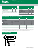
Parameter Symbol Test Conditions Min Typ Max Units
Operating Voltage Range,
V
SUPPLY
=[(V+)-(V-)]
V
SUPPLY
- 2 to 30 - V
Forward Voltage Drop
IN to V- V
FWDL
I
IN
=2A(Peak Pulse) - 2 - V
IN to V+ V
FWDH
- 2 - V
Input Leakage Current I
IN
-20 5 20 nA
Quiescent Supply Current I
QUIESCENT
- 50 200 nA
Equivalent SCR ON Threshod Note 3 - 1. 1 - V
Equivalent SCR ON Resistance V
FWD
/I
FWD
; Note 3 - 0.5 - Ω
Input Capacitance C
IN
- 5 - PF
Input Switching Speed t
ON
- 2 - ns
Note:
ESD Ratings and Capability (Figure 1, Table 1)
Load Dump and Reverse Battery (Note 2)
1. θ
JA
is measured with the component mounted on an evaluation PC board in free air.
Notes:
2. In automotive ans battery operated systems, the power supply lines should be externally protected for load dump and reverse battery. When the V+ and V- Pins are connected to the same
supply voltage source as the device or control line under protection, acurrent limiting resistor should be connectied in series between the external supply and the SP723 supply pins to
limit reverse battery current to within the rated maximum limits. Bypass capacitors of typically 0.01µF or larger from the V+ and V- Pins to ground are recommended.
3. Refer to the Figure 3 graph for determine peak current and dessipation under EOS conditions.
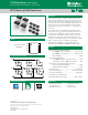
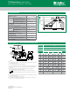
FIGURE 4. TYPICAL APPLICA TION OF THE SP723 AS AN INPUT CLAMP FOR OVER-VOLTAGE, GREATER THAN 1V
BE
ABOVE V+ OR
LESS THAN -1V
BE
BELOW V-
+V
CC
INPUT
DRIVERS
SP723 INPUT PROTECTION CIRCUIT (1 OF 6 SHO WN)
OR
SIGNAL
SOURCES
IN 5 - 7IN 1 - 3
SP723
V-
TO +V
CC
LINEAR OR
DIGITAL IC
INTERFAC E
V+
+V
CC
(Application as an Input Clamp for Over-voltage, Greater than 1V
BE
Above V+ or less than -1V
BE
below V-)
Typical Application of the SP723