
User Manual

© 2013 Littelfuse, Inc.
Specifications are subject to change without notice.
Revised: 04/24/13
TVS Diode Arrays (SPA
®
Diodes)
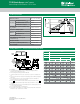
General Purpose ESD Protection - SP721 Series
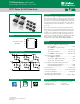
Part Numbering System
Lead Plating Matte Tin
Lead Material Copper Alloy
Lead Coplanarity 0.004 inches (0.102mm)
Substitute Material Silicon
Body Material Molded Epoxy
Flammability UL 94 V-0
Product Characteristics
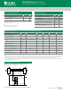
Ordering Information
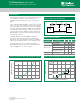
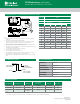
Package Dimensions — Small Outline Plastic Packages (SOIC)
Notes:
1. Symbols are defined in the “MO Series Symbol List” in Section 2.2 of Publication
Number 95.
2. Dimensioning and tolerancing per ANSI Y14.5M-1982.
3. Dimension “D” does not include mold flash, protrusions or gate burrs. Mold flash,
protrusion and gate burrs shall not exceed 0.15mm (0.006 inch) per side.
4. Dimension “E” does not include interlead flash or protrusions. Inter-lead flash and
protrusions shall not exceed 0.25mm (0.010 inch) per side.
5. The chamfer on the body is optional. If it is not present, a visual index feature must be
located within the crosshatched area.
6. “L” is the length of terminal for soldering to a substrate.
7. “N” is the number of terminal positions.
8. Terminal numbers are shown for reference only.
9. The lead width “B”, as measured 0.36mm (0.014 inch) or greater above the seating
plane, shall not exceed a maximum value of 0.61mm (0.024 inch).
10. Controlling dimension: MILLIMETER. Converted inch dimensions are not necessarily
exact.
Package SOIC
Pins 8
JEDEC MS-012
Millimeters Inches
Notes
Min Max Min Max
A 1.35 1.75 0.0532 0.0688 -
A1 0.10 0.25 0.0040 0.0098 -
B 0.33 0.51 0.013 0.020 9
C 0.19 0.25 0.0075 0.0098 -
D 4.80 5.00 0.1890 0.1968 3
E 3.80 4.00 0.1497 0.1574 4
e 1.27 BSC 0.050 BSC -
H 5.80 6.20 0.2284 0.2440 -
h 0.25 0.50 0.0099 0.0196 5
L 0.40 1.27 0.016 0.050 6
N 8 8 7
µ 0º 8º 0º 8º -
INDEX
AREA
E
D
N
123
-B-
0.25(0.010)CAM BS
e
-A-
L
B
M
-C-
A1
A
SEATING PLANE
0.10(0.004)
h x 45
o
C
H
0.25(0.010)BM M
NOTES:
1. Symbols are defined in the “MO Series Symbol List” in Section 2.2 of
Publication Number 95.
2. Dimensioning and tolerancing per ANSI Y14.5M-1982.
3. Dimension “D” does not include mold flash, protrusions or gate burrs.
Mold flash, protrusion and gate burrs shall not exceed 0.15mm (0.006
inch) per side.
4. Dimension “E” does not include interlead flash or protrusions. Inter-
lead flash and protrusions shall not exceed 0.25mm (0.010 inch) per
side.
5. The chamfer on the body is optional. If it is not present, a visual index
feature must be located within the crosshatched area.
6. “L” is the length of terminal for soldering to a substrate.
7. “N” is the number of terminal positions.
8. Terminal numbers are shown for reference only.
9. The lead width “B”, as measured 0.36mm (0.014 inch) or greater
above the seating plane, shall not exceed a maximum value of
0.61mm (0.024 inch).
10. Controlling dimension:MILLIMETER. Converted inch dimensions
are not necessarily exact.
μ
Part Number Temp. Range (ºC) Package
Environmental
Informaton
Marking Min. Order
SP721APP -40 to 105 8 Ld PDIP Lead-free SP721AP(P)
1
2000
SP721ABG -40 to 105 8 Ld SOIC Green SP721A(B)G
2
1960
SP721ABTG -40 to 105
8 Ld SOIC Tape
and Reel
Green SP721A(B)G
2
2500
SP 721
Series
Package
P = Lead Free
TG= Tape and Reel
AB = 8 Ld SOIC
AP = 8 Ld PDIP
G = Green
TVS Diode Arrays
(SPA
®
Diodes)
**
**
Notes:
1. SP721AP(P) means device marking either SP721AP or SP721APP.
2. SP721A(B)G means device marking either SP721AG or SP721ABG which are good for types SP721ABG and SP721ABTG.