
Datasheet


132
RoHS Compliant, ELV Compliant
HF
Halogen Free
12
Solder Reflow and Rework Recommendation for Surface-mount Devices
Classification Reflow Profiles
Solder Reflow
• Recommended reflow methods:
- IR
- Hot air
- Nitrogen
• Recommended maximum paste thickness: 0.25mm (0.010 inch)
• Devices can be cleaned using standard methods and aqueous solvents.
• We believe the optimum conditions for forming acceptable solder fillets occur when a reasonable amount of solder paste is placed
underneath each device’s termination. As such, we request that customers comply with our recommended solder pad layouts.
• Customer should validate that the solder paste amount and reflow recommendations meet its application.
• We request that customer board layouts refrain from placing raised features (e.g. vias, nomenclature, traces, etc.) underneath PolySwitch
devices. It is possible that raised features could negatively impact solderability performance of our devices.
Rework
• femtoSMD, picoSMD, nanoSMD, microSMD and miniSMD series: standard industry practices.
Please also avoid direct contact to the device.
• SMD series: rework should be confined to removal of the installed product and replacement with a fresh device.
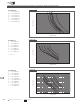
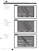
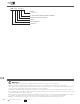
Profile Feature Pb-Free Assembly
Average ramp up rate (Ts
MAX
toTp) 3°C/second max.
Preheat
• Temperature min. (Ts
MIN
) 150°C
• Temperature max. (Ts
MAX
) 200°C
• Time (ts
MIN
to ts
MAX
) 60-120 seconds
Time maintained above:
• Temperature (T
L
) 217°C
• Time (t
L
) 60-150 seconds
Peak/Classification temperature (Tp) 260°C
Time within 5°C of actual peak temperature
Time (tp) 30 seconds max.
Ramp down rate 3°C/second max.
Time 25°C to peak temperature 8 minutes max.
Critical Zone
T
L
to Tp
Ramp up
t 25˚C to Peak
Reflow Profile
Time
Ramp down
ts
Preheat
Ts
MAX
T
L
Tp
tp
25
Ts
MIN
t
L
Temperature
Figure S14
Note: All temperatures refer to topside of the package, measured on the package
body surface.
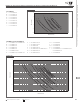
W 8.0 ± 0.30 8.0 ± 0.30 8.0 ± 0.30 8.0 ± 0.30 12.0 ± 0.30 24.0 ± 0.30 16.0 ± 0.30 16.0 ± 0.30 16.0 ± 0.30
P
0
4.0 ± 0.10 4.0 ± 0.10 4.0 ± 0.10 4.0 ± 0.10 4.0 ± 0.10 4.0 ± 0.10 4.0 ± 0.10 4.0 ± 0.10 4.0 ± 0.10
P
1
4.0 ± 0.10 4.0 ± 0.10 4.0 ± 0.10 4.0 ± 0.10 8.0 ± 0.10 8.0 ± 0.10 8.0 ± 0.10 8.0 ± 0.10 12.0 ± 0.10
P
2
2.0 ± 0.05 2.0 ± 0.05 2.0 ± 0.05 2.0 ± 0.05 2.0 ± 0.05 2.0 ± 0.10 2.0 ± 0.10 2.0 ± 0.10 2.0 ± 0.10
A
0
Table S8 Table S8 1.95 ± 0.10 2.9 ± 0.10 Table S8 5.70 ± 0.10 5.11 ± 0.15 5.6 ± 0.23 6.9 ± 0.23
B
0
Table S8 Table S8 Table S8 3.50 ± 0.10 Table S8 11.90 ± 0.10 5.6 ± 0.23 8.1 ± 0.15 9.6 ± 0.15
B
1
max. 4.35 4.35 4.35 4.35 8.2 20.1 12.1 12.1 12.1
D
0
1.55 ± .05 1.55 ± .05 1.55 ± .05 1.55 ± .05 1.5 + 0.10/ -.00 1.55 ± .05 1.5 + 0.10/ -.00 1.5 + 0.10/ -.00 1.5 + 0.10/ -.00
F 3.50 ± 0.05 3.50 ± 0.05 3.50 ± 0.05 3.50 ± 0.05 5.50 ± 0.05 11.50 ± 0.10 7.50 ± 0.10 7.50 ± 0.10 7.50 ± 0.10
E
1
1.75 ± 0.10 1.75 ± 0.10 1.75 ± 0.10 1.75 ± 0.10 1.75 ± 0.10 1.75 ± 0.10 1.75 ± 0.10 1.75 ± 0.10 1.75 ± 0.10
E
2
min. 6.25 6.25 6.25 6.25 10.25 22.25 14.25 14.25 14.25
T max. 0.6 0.6 0.6 0.6 0.6 0.6 0.6 0.6 0.6
T
1
max. 0.1 0.1 0.1 0.1 0.1 0.1 0.1 0.1 0.1
K
0
Table S8 Table S8 Table S8 Table S8 Table S8 0.95 ± 0.10 1.8 ± 0.15 3.2 ± 0.15 3.4 ± 0.15
Leader min. 390 390 390 390 390 400 400 400 400
Trailer min. 160 160 160 160 160 160 160 160 160
Description
nanoSMDC
EIA 481-1
microSMD
EIA 481-1
miniSMDC
and
decaSMDC050F/60
EIA 481-1
miniSMDE190
EIA 481-2
midSMD
except
decaSMDC050F/60
EIA 481-2
SMD
EIA 481-2
SMD2
EIA 481-2
picoSMDC
EIA 481-1
femtoSMDC
EIA 481-1
Table S7 Tape and Reel Specifications for Surface-mount Devices (in Millimeters)