
Installation Guide

LED Lighting Surge Protection Modules
Design and Installation Guide
© 2016 Littelfuse • LED Lighting SPD Module Design and Installation Guide www.littelfuse.com
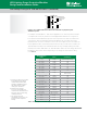
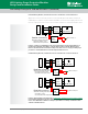
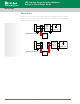
The following steps summarize a design process that helps ensure enough inductance is
present between the SPD MOVs and the one in the driver:
1. MOV1 and MOV2 need to be coordinated so that most of surge current/energy flows
through MOV1.
2. Select MOVs with V
M
of MOV1 ≤ V
M
of MOV2, where V
M
is the Maximum Continuous
Operating Voltage.
3. Select MOVs with V
C
of MOV1 ≤ V
C
of MOV2, where V
C
is the Maximum
Clamping Voltage.
4. V
MOV1
= V
MOV2
+ L (di/dt)
5. Inductance L may be added in series with the SPD. Increasing inductance L will result in
better coordination as MOV1 absorbs the higher surge energy
6. Refer to the embedded links in the SPD blocks of Figure 17 for MOV technical
information. See the Littelfuse Varistor Ordering Information Diagram for details on
constructing a part number.
The Littelfuse Application Team has years of expertise in such coordination requirements and
has helped many customers optimize their circuit reliability while meeting surge immunity
requirements.
Power Supply Unit Design Considerations (Fuse, Equivalent
Resistance, TVS Diode)
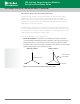
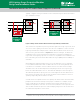
Although an SPD module is designed to absorb most of the surge energy produced by
a lightning strike, some residual energy can enter the LED driver and cause damage to
the components inside it (Figure 18). To minimize the damage, always consider an LED
driver design that works in cooperation with the SPD module so less energy can enter the
LED driver.
Power Supply Unit Design Considerations
18