USER MANUAL BLE Bluetooth Module WB100N Version 1.1 Author: Kaysa Lee Change History Revision Version 1.0 Version 1.1 Date 2017/01/06 2017/03/22 Author Kaysa Lee Kaysa Lee Change List Preliminary IC use 1802 and update features * This document contains confidential proprietary information and is property of LTC. The contents of this document should not be disclosed to unauthorized persons without the written consent of LTC.
CONTENT PRODUCT FEATURES .................................................................................................................... 3 PRODUCT SPECIFICATIONS ........................................................................................................ 3 MAIN CHIPSET ....................................................................................................................................... 3 FUNCTIONAL SPECIFICATIONS .............................................................
Product Features LiteON BLE Module WB100N 是一款採用 nRF51802 為核心處理器的高性能、低功耗 (Bluetooth Low Energy)的射頻收發系統模組,擁有超小體積封裝,整體尺寸為 14.3*14.3mm 支持完整的低功耗藍牙 4.0 協議,以及支持藍牙 4.
• 250 kbps, 1 Mbps, 2 Mbps supported data rates • TX Power -20 to +4 dBm in 4 dB steps • TX Power -35 dBm Whisper mode • 13 mApeak RX, 10.5 mApeak TX (0 dBm) • 10 mApeak RX, 8 mApeak TX (0 dBm) with DC/DC • RSSI (1 dB resolution) • ARMR Cortex™-M0 32 bit processor • Serial Wire Debug (SWD) • S100 series SoftDevice ready • Memory • 256 kB embedded flash program memory • 16 kB RAM • On-air compatibility with nRF24L series • Flexible Power Management •Supply voltage range 1.8 V to 3.6 V • 7.
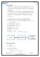
PRODUCT PICTURE Module: WB100N Specification Page 5/9 LTC Network Access Confidential 2017/9/19
PIN ASSIGNMENT PIN 1 2 3 4 5 6 7 8 9 10 11 12 13 Name/Function VDD/Power supply General purpose I/O pin General purpose I/O pin General purpose I/O pin General purpose I/O pin General purpose I/O pin General purpose I/O pin General purpose I/O pin General purpose I/O pin General purpose I/O pin General purpose I/O pin General purpose I/O pin General purpose I/O pin WB100N Specification Page 6/9 LTC Network Access Confidential Remark P0.30 P0.00 P0.01 P0.02 P0.03 P0.04 P0.05 P0.06 P0.07 P0.08 P0.09 P0.
14 15 16 17 18 19 20 General purpose I/O pin General purpose I/O pin General purpose I/O pin General purpose I/O pin General purpose I/O pin General purpose I/O pin SWDIO nRESET/System reset (active low). Also hardware debug and flash programming I/O. 21 SWDCLK/Hardware debug and flash programming I/O.
FCC WARING STATEMENT FEDERAL COMMUNICATIONS COMMISSION INTERFERENCE STATEMENT This equipment has been tested and found to comply with the limits for a Class B digital device, pursuant to Part 15 of the FCC Rules. These limits are designed to provide reasonable protection against harmful interference in a residential installation.
2. The host manufacturer is responsible for additional testing to verify compliance as a composite system. When testing the host device for compliance with the Part 15 Subpart B requirements, the host manufacturer is required to show compliance with the Part 15 Subpart B while the transmitter module(s) are installed and operating. The modules should be transmitting and the evaluation should confirm that the module’s intentional emissions are compliant (i.e.