
Data Sheet

LILY-W1 series - Data sheet
UBX-15000203 - R12 Electrical specifications Page 15 of 42
C1-Public
4 Electrical specifications
Stressing the device above one or more of the Absolute maximum ratings can cause permanent
damage. These are stress ratings only. Operating the module at these or at any conditions other
than those specified in the Operating conditions should be avoided. Exposure to absolute
maximum rating conditions for extended periods may affect device reliability.
Where application information is given, it is advisory only and does not form part of the
specification.
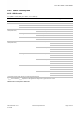
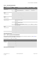
4.1 Absolute maximum ratings
Symbol Description Condition Min Max Unit
VCC Module supply voltage Input DC voltage at VCC pin - 4.0 V
VCC_IO IO voltage supply Input DC voltage at VCC_IO pin 1.8 V mode - 2.2 V
3.3 V mode 4.0 V
Table 5: Absolute maximum ratings
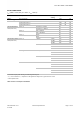
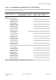
4.1.1 Maximum ESD ratings
Applicability Immunity level Unit
All pins except
ANT
Human Body Model (HBM), ANSA/ESDA/JEDEC JS-001-2014.
±
2000 V
Charged Device Model (CDM), JESD22-C101.
±
500 V
ANT pin and
Internal
antenna
Human Body Model (HBM), ANSA/ESDA/JEDEC JS-001-2014.
±
300 V
Charged Device Model (CDM), JESD22-C101.
±
600 V
Table 6: Maximum ESD ratings
4.2 Operating conditions
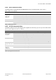
4.2.1 Temperature range
Parameter Min Max
Unit
Storage temperature -40 +85 °C
Operating temperature -40 +85 °C
Table 7: Temperature range
4.2.2 Power supply
Read the Safety compliance notice before using the modules.
Symbol Parameter Min. Typ. Max. Unit
VCC Supply voltage 3.00 3.30 3.60 V
VCC_IO Digital IO supply
voltage
1.8 V mode 1.62 1.80 1.98 V
3.3 V mode 3.00 3.30 3.60 V
Table 8: Power supply voltage