
User's Manual

Data Sheet: CR Series
JukeBlox Networked Media Modules
dat_CR860_CR870_3_5_datasheet_b.doc CONFIDENTIAL Version 3.5 – May 15
th
2011 - Page 21 of 26
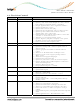
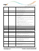
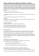
J1 – LCD Connector
Function GPIO IC PIN Signal Signal IC PIN GPIO Function
GND
12
GND
Y7 LCDD0
34
LCDD1 W7
V7 LCDD2
56
LCDD3 Y6
W6 LCDD4
78
LCDD5 V6
U6 LCDD6
910
LCDD7 Y5
W5 LCDD8
11 12
LCDD9 V5
U5 LCDD10
13 14
LCDD11 Y4
W4 LCDD12
15 16
LCDD13 V4
U4 LCDD14
17 18
LCDD15 Y3
W3 LCDD16
19 20
LCDD17 Y2
GND
21 22
GND
Y9 LCDCLK
23 24
LCDCTRL0 W9
Y8 LCDCTRL1
25 26
LCDCTRL2 W8
V8 LCDCTRL3
27 28
GND
GND
29 30
GND
PIN Number
LCD Interface
LCD Interface
LCD Interface
LCD Interface
Note: The IC PIN column indicates the pin number on the DM860 or DM870 integrated
circuit. This allows for easy cross-reference to the DM860 or DM870 data sheet
information.
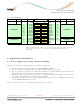
9. Application Guidelines
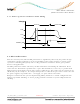
9.1 Power Supply sequencing and Reset Timing
There are strict power sequencing and reset timing requirements.
Power up the I/O voltage (3.3V) first and hold NRESET_MOD low.
The core voltage (1.2V) must never be higher than (I/O voltage +0.5 V).
The core voltage (1.2V) must be within the specified core voltage limits less than 300ms after
the I/O voltage (3.3V) reaches the specified I/O voltage limits.
Throughout the power down process, the 3.3V supply must maintain a higher voltagethan the
1.2V supply, until both have reached ground potential.
To assure a proper IC reset, the power supplies must be present for a minimum time of 2ms
before NRESET_MOD is de-asserted.
Please see the power and reset timing figure in Section 9.1.1 below.