
Datasheet


LTC3861
18
3861fa
For more information www.linear.com/LTC3861
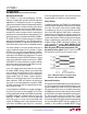
Figure 5. Oscillator Frequency vs R
FREQ
applicaTions inFormaTion
amplifier of the LTC3861 has a gain bandwidth of 40MHz,
high enough not to affect main loop compensation and
transient behavior. To avoid noise coupling into VSNSP,
the resistor divider should be placed near the VSNSP
and VSNSN pins and physically close to the LTC3861.
The remote output and ground traces should be routed
parallel to each other as a differential pair to the remote
output. These traces should be terminated as close as
physically possible to the remote output point that is to be
accurately regulated through remote differential sensing.
In addition, avoid routing these sensitive traces near any
high speed switching nodes in the circuit. Ideally, they
should be shielded by a low impedance ground plane to
maintain signal integrity.
Programming the Operating Frequency
The LTC3861 can be hard wired to one of two fixed fre-
quencies, linearly
programmed to any frequency between
250kHz and 2.25MHz or synchronized to an external clock.
Table 1 in the Operation section shows how to connect the
CLKIN and FREQ pins to choose the mode of frequency
programming. The frequency of operation is given by the
following equation:
Frequency = (R
FREQ
– 17kΩ) • 29Hz/Ω
Figure 5 shows operating frequency vs R
FREQ
.
Frequency Synchronization
The LTC3861 incorporates an internal phase-locked loop
(PLL) which enables synchronization of the internal os-
cillator (rising edge
of PWM1) to an external clock from
250kHz to 2.25MHz.
Since the entire PLL is internal to the LTC3861, simply
applying a CMOS level clock signal to the CLKIN pin will
enable frequency synchronization. A resistor from FREQ
to GND is still required to set the free running frequency
close to the sync input frequency.
Choosing the Inductor and Setting the Current Limit
The inductor value is related to the switching frequency,
which is chosen based on the trade-offs discussed in the
Operation section. The inductor can be sized using the
following equation:
L
V
fI
V
V
OUT
L
OUT
IN
=
⎛
⎝
⎜
⎞
⎠
⎟
−
⎛
⎝
⎜
⎞
⎠
⎟
•
•
Δ
1
Choosing a larger value of ∆I
L
leads to smaller L, but re-
sults in greater core loss (and higher output voltage ripple
for
a given output capacitance and/or ESR). A reasonable
starting point for setting the ripple current is 30% of the
maximum output current, or:
∆I
L
= 0.3 • I
OUT
The inductor saturation current rating needs to be higher
than the peak inductor current during transient condi-
tions. If
I
OUT
is the maximum rated load current, then
the maximum transient current, I
MAX
, would normally be
chosen to be some factor (e.g., 60%) greater than I
OUT
:
I
MAX
= 1.6 • I
OUT
The minimum saturation current rating should be set to
allow margin due to manufacturing and temperature varia-
tion in
the sense resistor or inductor DCR. A reasonable
value would be:
I
SAT
= 2.2 • I
OUT
R
FREQ
(kΩ)
0
OSCILLATOR FREQUENCY (MHz)
40
80
100
3861 F05
0.9
2.1
2.3
2.5
0.5
1.7
1.3
0.7
1.9
0.1
0.3
1.5
1.1
20
60
120