
Datasheet


LTC3861
13
3861fa
For more information www.linear.com/LTC3861
turned on for 20ns every eight cycles to allow the driver IC
to recharge its topside gate drive capacitor. The negative
OC threshold is equal to –3/4 the positive OC threshold.
See the Applications Information section for guidelines
on setting these thresholds.
Excellent Transient Response
The LTC3861 error amplifiers are true operational ampli-
fiers, meaning that
they have high bandwidth, high DC gain,
low offset and low output impedance. Their bandwidth,
when combined with high switching frequencies and low-
value inductors, allows the compensation network to be
optimized for very high control loop crossover frequencies
and excellent transient response. The 600mV internal ref-
erence allows regulated output voltages as low as 600mV
without external level-shifting amplifiers.
Line Feedforward Compensation
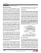
The LTC3861 achieves outstanding line transient response
using a feedforward correction scheme which instanta-
neously adjusts the duty cycle to compensate for changes
in input voltage, significantly reducing output overshoot
and undershoot. It has the added advantage of making
the DC loop gain independent of input voltage. Figure 2
shows how large transient steps at the input have little
effect on the output voltage.
The noninverting input of the differential amplifier is con-
nected to the midpoint of the feedback resistive divider
between
the positive and negative output capacitor ter-
minals. The
VSNSOUT is connected to the FB pin and the
amplifier
will attempt to regulate this voltage to 0.6V. The
amplifier is configured for unity gain, meaning that the
differential voltage between V
SNSP
and V
SNSN
is translated
to V
SNSOUT
, relative to SGND.
Shutdown Control Using the RUN Pins
The two channels of the LTC3861 can be independently
enabled using the RUN1 and RUN2 pins. When both pins
are driven low, all internal circuitry, including the internal
reference and oscillator, are completely shut down. When
the RUN pin is low, the respective COMP pin is actively
pulled down to ground. In a multiphase operation when
the COMP pins are tied together, the COMP pin is held
low until all the RUN pins are enabled. This ensures a
synchronized start-up of all the channels. A 1.5μA pull-up
current is provided for each RUN pin internally. The RUN
pins remain high impedance up to V
CC
.
Undervoltage Lockout
To prevent operation of the power supply below safe in
-
put voltage levels, both channels are disabled when V
CC
is below the undervoltage lockout (UVLO) threshold
(2.9V falling, 3V rising). If
a RUN pin
is driven high,
the LTC3861 will start up the reference to detect when
V
CC
rises above the UVLO threshold, and enable the
appropriate channel.
Overvoltage Protection
If the output voltage rises to more than 10% above the
set regulation value, which is reflected as a V
FB
voltage of
0.66V or above, the LTC3861 will force the PWM output
low to turn on the bottom MOSFET and discharge the
output. Normal operation resumes once the output is
back within the regulation window. However, if the re
-
verse current
flowing from V
OUT
back through the bottom
power MOSFET to PGND is greater than 3/4 the positive
OC threshold, the NOC comparator trips and shuts off the
bottom power MOSFET to protect it from being destroyed.
This scenario can happen when the LTC3861 tries to start
into a precharged load higher than the OV threshold. As
operaTion
(Refer to Functional Diagram)
Figure 2
Remote Sense Differential Amplifier
The LTC3861 includes two low offset, unity gain, high
bandwidth differential amplifiers for differential output
sensing. Output voltage accuracy is significantly improved
by removing board interconnection losses from the total
error budget.
20µs/DIV
38611 F02
V
IN
10V/DIV
V
OUT
50mV/DIV
AC-COUPLED
V
IN
= 7V TO 14V IN 20µs
V
OUT
= 1.2V
I
LOAD
= 20A
f
SW
= 300kHz
I
L1
10A/DIV
I
L2
10A/DIV