
Datasheet


LTC3861
12
3861fa
For more information www.linear.com/LTC3861
operaTion
(Refer to Functional Diagram)
Main Control Architecture
The LTC3861 is a dual-channel/dual-phase, constant-
frequency, voltage mode controller for DC/DC step-down
applications. It is designed to be used in a synchronous
switching architecture with external integrated-driver MOS
-
FETs or
power
blocks, or external drivers and N-channel
MOSFETs using single wire three-state PWM interfaces.
The controller allows the use of sense resistors or lossless
inductor DCR current sensing to maintain current balance
between phases and to provide overcurrent protection. The
operating frequency is selectable from 250kHz to 2.25MHz.
To multiply the effective switching frequency, multiphase
operation can be extended to 3, 4, 6, or 12 phases by paral
-
leling up
to
six controllers. In single or 3-phase operation, the
2nd or 4th channel can be used as an independent output.
The output voltage is resistively divided externally to
create a feedback voltage for the controller. Connect
VSNSP of the unity-gain internal differential amplifier,
DA, to the center tap of the feedback divider across the
output load, and VSNSN to the load ground. The output
of the differential amplifier VSNSOUT produces a signal
equal to the differential voltage sensed across VSNSP
and VSNSN. This scheme overcomes
any ground offsets
between
local ground and remote output ground, result-
ing in a more accurate output voltage.
In the main voltage mode control loop, the error ampli-
fier output (
COMP) directly controls the converter duty
cycle in order to drive the FB pin to 0.6V in steady state.
Dynamic changes in output load current can perturb the
output voltage. When the output is below regulation,
COMP rises, increasing the duty cycle. If the output rises
above regulation, COMP will decrease, decreasing the
duty cycle. As the output approaches regulation, COMP
will settle to the steady-state value representing the step-
down conversion ratio.
In normal operation, the PWM latch is set high at the begin
-
ning of the clock cycle (assuming COMP > 0.5V). When
the
(line feedforward compensated) PWM ramp exceeds
the COMP voltage, the comparator trips and resets the
PWM latch. If COMP is less than 0.5V at the beginning
of the clock cycle, as in the case of an overvoltage at the
outputs, the PWM pin remains low throughout the entire
cycle. When the PWM pin goes high it has a minimum
on-time of approximately 20ns and a minimum off-time
of approximately one-twelth the
switching period.
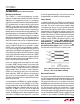
Current Sharing
In multiphase operation, the LTC3861 also incorporates an
auxiliary current sharing loop. Inductor current is sampled
each cycle. The master’s current sense amplifier output
is averaged at the I
AVG
pin. A small capacitor connected
from I
AVG
to GND (typically 100pF) stores a voltage cor-
responding to
the instantaneous average current of the
master. Each phase integrates the difference between its
current and the master’s. Within each phase the integrator
output is proportionally summed with the system error
amplifier voltage (COMP), adjusting that phase’s duty
cycle to equalize the currents. When multiple ICs are
daisychained the I
AVG
pins must be connected together.
When the phases are operated independently, the I
AVG
pin should be tied to ground. Figure 1 shows a transient
load step with current sharing in a 3-phase system.
Figure 1. Mismatched Inductor Load Step Transient
Response (3-Phase Using FDMF6707B DrMOS)
Overcurrent Protection
The current sense amplifier outputs also connect to overcur-
rent (OC) comparators that provide fault protection in the
case of an output short. When an OC fault is detected for
128 consecutive clock cycles, the controller three-states
the PWM output, resets the soft-start capacitor, and waits
for 32768 clock cycles before attempting to start up again.
The 128 consecutive clock cycle counter has a 7-cycle
hysteresis window, after which it will reset. The LTC3861
also provides negative OC (NOC) protection by preventing
turn-on of the bottom MOSFET during a negative OC fault
condition. In this condition, the bottom MOSFET will be
50µs/DIV
3861 F01
V
OUT
100mV/DIV
AC-COUPLED
V
IN
= 12V
V
OUT
= 1V
I
LOAD
STEP = 0A TO 30A TO 0A
f
SW
= 500kHz EXTERNAL CLOCK
I
L1 (L= 0.47µH)
10A/DIV
I
L2 (L= 0.25µH)
10A/DIV
I
L3 (L= 0.47µH)
10A/DIV