
Datasheet


LTC3788
22
3788fc
applicaTions inForMaTion
Table 2 summarizes the different states in which the FREQ
pin can be used.
Table 2.
FREQ PIN PLLIN/MODE PIN FREQUENCY
0V DC Voltage 350kHz
INTV
CC
DC Voltage 535kHz
Resistor DC Voltage 50kHz to 900kHz
Any of the Above External Clock Phase Locked to
External Clock
Minimum On-Time Considerations
Minimum on-time, t
ON(MIN)
, is the smallest time duration
that the LTC3788 is capable of turning on the bottom
MOSFET. It is determined by internal timing delays and
the gate charge required to turn on the top MOSFET. Low
duty cycle applications may approach this minimum on-
time limit.
In forced continuous mode, if the duty cycle falls below
what can be accommodated by the minimum on-time,
the controller will begin to skip cycles but the output will
continue to be regulated. More cycles will be skipped when
V
IN
increases. Once V
IN
rises above V
OUT
, the loop works
to keep the top MOSFET on continuously. The minimum
on-time for the LTC3788 is approximately 110ns.
Efficiency Considerations
The percent efficiency of a switching regulator is equal to
the output power divided by the input power times 100%.
It is often useful to analyze individual losses to determine
what is limiting the efficiency and which change would
produce the greatest improvement. Percent efficiency can
be expressed as:
%
Efficiency = 100% – (L1 + L2 + L3 + ...)
where
L1, L2, etc., are the individual losses as a percent-
age of input power.
Although all dissipative elements in the circuit produce
losses, four main sources usually account for most of the
losses in LTC3788 circuits: 1) IC V
IN
current, 2) INTV
CC
regulator current, 3) I
2
R losses, 4) Bottom MOSFET
transition losses.
1. The V
IN
current is the DC supply current given in the
Electrical Characteristics table, which excludes MOSFET
driver and control currents. V
IN
current typically results
in a small (<0.1%) loss.
2. INTV
CC
current is the sum of the MOSFET driver and
control currents. The MOSFET driver current results
from switching the gate capacitance of the power MOS-
FETs. Each time a MOSFET gate is switched from low to
high to low again, a packet of charge, dQ, moves from
INTV
CC
to ground. The resulting dQ/dt is a current out
of INTV
CC
that is typically much larger than the control
circuit current. In continuous mode, I
GATECHG
= f(Q
T
+
Q
B
), where Q
T
and Q
B
are the gate charges of the topside
and bottom side MOSFETs.
3. DC I
2
R losses. These arise from the resistances of the
MOSFETs, sensing resistor, inductor and PC
board traces
and cause the efficiency to drop at high output currents.
4. Transition losses apply only to the bottom MOSFET(s),
and become significant only when operating at low
input voltages. Transition losses can be estimated from:
Transition Loss = (1.7)
V
OUT
3
V
IN
I
O(MAX)
• C
RSS
f
Other hidden losses, such as copper trace and internal
battery resistances, can account for an additional 5% to
10% efficiency degradation in portable systems. It is very
important to include these system-level losses during the
design phase.
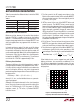
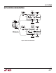
Figure 6. Relationship Between Oscillator
Frequency and Resistor Value at the FREQ Pin
FREQ PIN RESISTOR (kΩ)
15
FREQUENCY (kHz)
600
800
1000
35 45 5525
3788 F06
400
200
500
700
900
300
100
0
65 75 85 95 105 115
125