
Datasheet
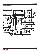


LTC3788
18
3788fc
applicaTions inForMaTion
specification for the MOSFETs as well; many of the logic
level MOSFETs are limited to 30V or less.
Selection criteria for the power MOSFETs include the
on-resistance R
DS(ON)
, Miller capacitance C
MILLER
, input
voltage and maximum output current. Miller capacitance,
C
MILLER
, can be approximated from the gate charge curve
usually provided on the MOSFET manufacturer’s data
sheet. C
MILLER
is equal to the increase in gate charge
along the horizontal axis while the curve is approximately
flat divided by the specified change in V
DS
. This result is
then multiplied by the ratio of the application applied V
DS
to the gate charge curve specified V
DS
. When the IC is
operating in continuous mode, the duty cycles for the top
and bottom MOSFETs are given by:
Main SwitchDuty Cycle =
V
OUT
−
V
IN
V
OUT
Synchronous SwitchDuty Cycle =
V
IN
V
OUT
The MOSFET power dissipations at maximum output
current are given by:
P
MAIN
=
(V
OUT
−
V
IN
)V
OUT
V
2
IN
•I
OUT(MAX)
2
• 1+ δ
( )
• R
DS(ON)
+k • V
3
OUT
•
I
OUT(MAX)
V
IN
• R
DR
• C
MILLER
• f
P
SYNC
=
V
IN
V
OUT
•I
OUT(MAX)
2
• 1+ δ
( )
• R
DS(ON)
where d is the temperature dependency of R
DS(ON)
and
R
DR
(approximately 1Ω) is the effective driver resistance
at the MOSFET’s Miller threshold voltage. The constant k,
which accounts for the loss caused by reverse recovery
current, is inversely proportional to the gate drive current
and has an empirical value of 1.7.
Both MOSFETs have I
2
R losses while the bottom N-channel
equation includes an additional term for transition losses,
which are highest at low input voltages. For high V
IN
the
high current efficiency generally improves with larger
MOSFETs, while for low V
IN
the transition losses rapidly
increase to the point that the use of a higher R
DS(ON)
device
with lower C
MILLER
actually provides higher efficiency.
The synchronous MOSFET losses are greatest at high
input voltage when the bottom switch duty factor is low
or during overvoltage when the synchronous switch is on
close to 100% of the period.
The term (1+ d) is generally given for a MOSFET in the
form of a normalized R
DS(ON)
vs Temperature curve, but
d = 0.005/°C can be used as an approximation for low
voltage MOSFETs.
C
IN
and C
OUT
Selection
The input ripple current in a boost converter is relatively
low (compared with the output ripple current), because this
current is continuous. The input capacitor C
IN
voltage rating
should comfortably exceed the maximum input voltage.
Although ceramic capacitors can be relatively tolerant of
overvoltage conditions, aluminum electrolytic capacitors
are not. Be sure to characterize the input voltage for any
possible overvoltage transients that could apply excess
stress to the input capacitors.
The value of the C
IN
is a function of the source impedance,
and in general, the higher the source impedance, the higher
the required input capacitance. The required amount of
input capacitance is also greatly affected by the duty cycle.
High output current applications that also experience high
duty cycles can place great demands on the input supply,
both in terms of DC current and ripple current.
In a boost converter, the output has a discontinuous current,
so C
OUT
must be capable of reducing the output voltage
ripple. The effects of ESR (equivalent series resistance)
and the bulk capacitance must be considered when choos-
ing the right capacitor for a given output ripple voltage.
The steady ripple voltage due to charging and discharging
the bulk capacitance is given by:
V
RIPPLE
=
I
OUT(MAX)
• (V
OUT
− V
IN(MIN)
)
C
OUT
• V
OUT
• f
V
where C
OUT
is the output filter capacitor.
The steady ripple due to the voltage drop across the ESR
is given by:
∆V
ESR
= I
L(MAX)
• ESR