
Datasheet


Table Of Contents
- Features
- Applications
- Description
- Typical Application
- Absolute Maximum Ratings
- Pin Configuration
- Order Information
- Electrical Characteristics
- Typical Performance Characteristics
- Pin Functions
- Functional Diagram
- Operation
- Applications Information
- Typical Applications
- Package Description
- Revision History
- Typical Application
- Related Parts
LTC3608
4
3608fc
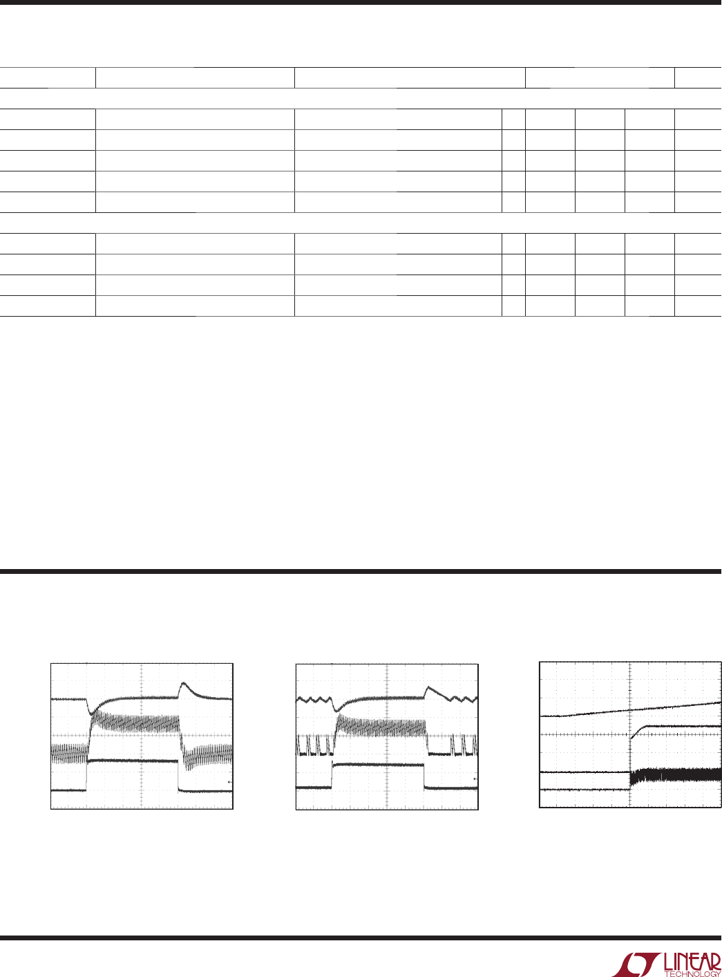
Transient Response
Transient Response
Start-Up
V
IN
= 12V
V
OUT
= 2.5V
R
LOAD
= 0.5Ω
FIGURE 6 CIRCUIT
3608 G03
40ms/DIV
RUN/SS
2V/DIV
V
OUT
1V/DIV
I
L
5A/DIV
Note 1: Stresses beyond those listed under Absolute Maximum Ratings
may cause permanent damage to the device. Exposure to any Absolute
Maximum Rating condition for extended periods may affect device
reliability and lifetime.
Note
2: T
J
is calculated from the ambient temperature T
A
and power
dissipation P
D
as follows:
T
J
= T
A
+ (P
D
• 29°C/W)(θ
JA
is simulated per JESD51-7 high effective
thermal conductivity test board)
θ
JC
= 1°C/W (θ
JC
is simulated when heat sink is applied at the bottom
of the package.)
Note 3:
The LTC3608 is tested in a feedback loop that adjusts V
FB
to
achieve a specified error amplifier output voltage (I
TH
). The specification at
85°C is not tested in production. This specification is assured by design,
characterization, and correlation to testing at 125°C.
Note
4: The LTC3608 is tested under pulsed load conditions such that
T
J
≈ T
A
. The LTC3608E is guaranteed to meet specifications from
0°C to 125°C junction temperature. Specifications over the –40°C to
125°C operating junction temperature range are assured by design,
characterization and correlation with statistical process controls. The
LTC3608I is guaranteed over the full –40°C to 125°C operating junction
temperature range. Note that the maximum ambient temperature
consistent with these specifications is determined by specific operating
conditions in conjunction with board layout, the rated package thermal
impedance and other environmental factors.
typical perForMance characteristics
SYMBOL PARAMETER CONDITIONS MIN TYP MAX UNITS
Internal V
CC
Regulator
V
INTVCC
Internal V
CC
Voltage 6V < V
IN
< 18V, V
EXTVCC
= 4V
l
4.7 5 5.5 V
ΔV
LDO(LOADREG)
Internal V
CC
Load Regulation I
CC
= 0mA to 20mA, V
EXTVCC
= 4V –0.1 ±2 %
V
EXTVCC
EXTV
CC
Switchover Voltage I
CC
= 20mA, V
EXTVCC
Rising
l
4.5 4.7 V
ΔV
EXTVCC
EXTV
CC
Switch Drop Voltage I
CC
= 20mA, V
EXTVCC
= 5V 150 300 mV
ΔV
EXTVCC(HYS)
EXTV
CC
Switchover Hysteresis 500 mV
PGOOD Output
ΔV
FBH
PGOOD Upper Threshold V
FB
Rising 7 10 13 %
ΔV
FBL
PGOOD Lower Threshold V
FB
Falling –7 –10 –13 %
ΔV
FB(HYS)
PGOOD Hysteresis V
FB
Returning 1 2.5 %
V
PGL
PGOOD Low Voltage I
PGOOD
= 5mA 0.15 0.4 V
LOAD STEP 0A TO 8A
V
IN
= 12V
V
OUT
= 2.5V
FCB = 0V
FIGURE 6 CIRCUIT
3608 G01
20µs/DIV
V
OUT
200mV/DIV
I
L
5A/DIV
I
LOAD
5A/DIV
V
IN
= 12V
V
OUT
= 2.5V
FCB = INTV
CC
FIGURE 6 CIRCUIT
3610 G02
20µs/DIV
V
OUT
200mV/DIV
I
L
5A/DIV
I
LOAD
5A/DIV
electrical characteristics
The l denotes the specifications which apply over the full operating
junction temperature range, otherwise specifications are at T
A
= 25°C. V
IN
= 15V unless otherwise noted.