
Datasheet


Table Of Contents
- Features
- Applications
- Description
- Typical Application
- Absolute Maximum Ratings
- Pin Configuration
- Order Information
- Electrical Characteristics
- Typical Performance Characteristics
- Pin Functions
- Functional Diagram
- Operation
- Applications Information
- Typical Applications
- Package Description
- Revision History
- Typical Application
- Related Parts
LTC3608
18
3608fc
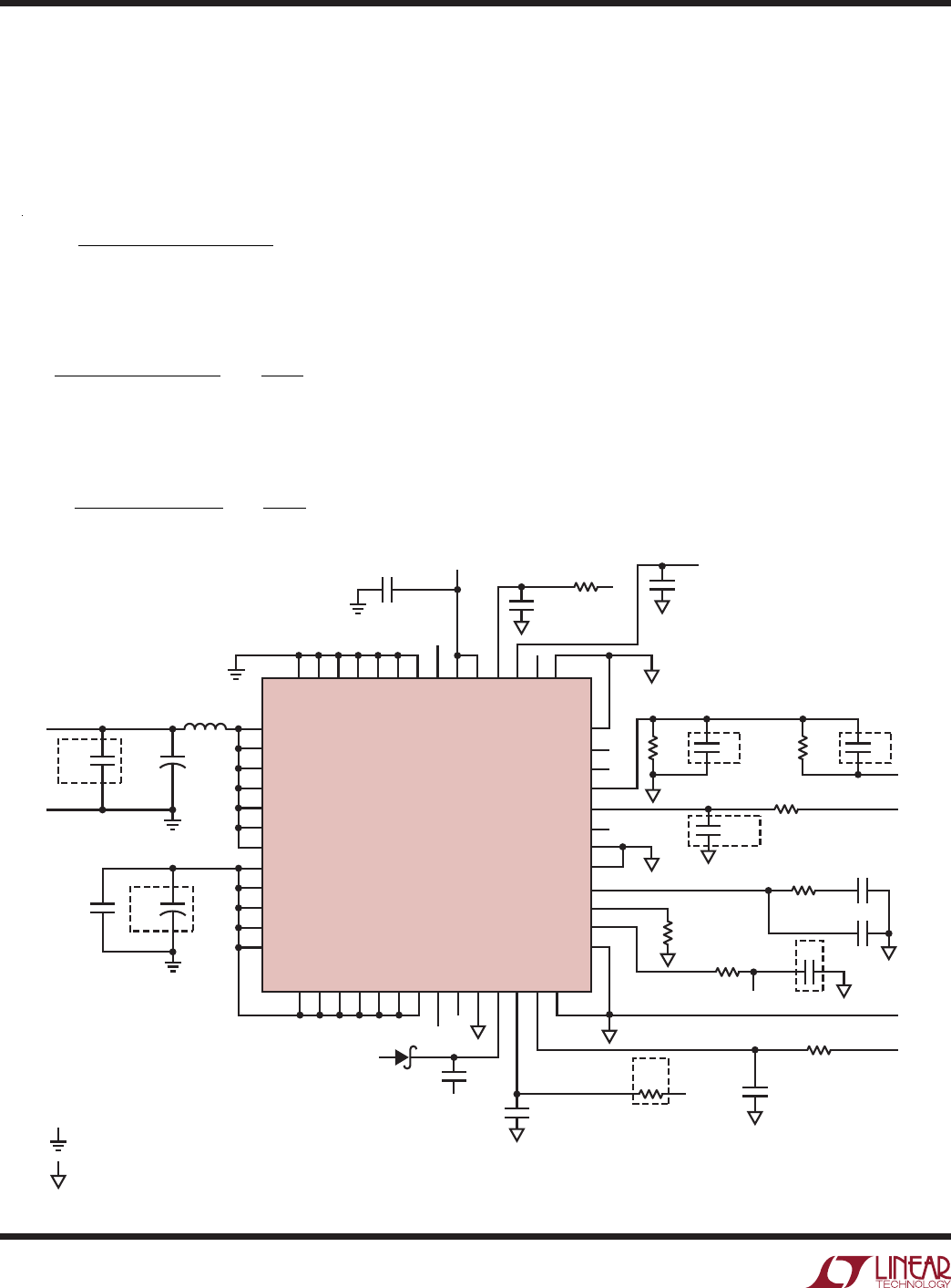
Figure 6. Design Example: 5V to 18V Input to 2.5V/8A at 550kHz
applications inForMation
Design Example
As a design example, take a supply with the following
specifications: V
IN
= 5V to 20V (12V nominal), V
OUT
=
2.5V ±5%, I
OUT
= 8A, f = 550kHz. First, calculate the tim-
ing resistor with V
ON
= V
OUT
:
R
ON
=
2.5V
550kHz
( )
10pF
( )
(2.4V)
≈ 187k
and choose the inductor for about 40% ripple current at
the maximum V
IN
:
L =
2.5V
550kHz
( )
0.4
( )
8A
( )
1−
2.5V
20V
⎛
⎝
⎜
⎞
⎠
⎟
= 1.24µH
Selecting a standard value of 1.2µH results in a maximum
ripple current of:
ΔI
L
=
2.5V
550kHz
( )
1.2µH
( )
1 –
2.5V
12V
⎛
⎝
⎜
⎞
⎠
⎟
= 3A
Next, set up V
RNG
voltage and check the I
LIMIT
. Tying V
RNG
to 0.5V will set the typical current limit to 11A, and tying
V
RNG
to GND will result in a typical current around 16A.
C
IN
is chosen for an RMS current rating of about 5A at
85°C. The output capacitors are chosen for a low ESR
of 0.002Ω to minimize output voltage changes due to
inductor ripple current and load steps. The ripple voltage
will be only:
ΔV
OUT(RIPPLE)
= ΔI
L(MAX)
(ESR)
= (3A) (0.002Ω) = 6mV
However, a 0A to 8A load step will cause an output change
of up to:
ΔV
OUT(STEP)
= ΔI
LOAD
(ESR) = (8A) (0.002Ω) = 16mV
An optional 22µF ceramic output capacitor is included
to minimize the effect of ESL in the output ripple. The
complete circuit is shown in Figure 6.
EXTV
CC
C4
0.01µF
C
IN
: TAIYO YUDEN GMK325BJ106MM-B
C
OUT
: TDKC2012X5ROJ226M
L1: CDEP85NP-R80MC-50
C5: MURATA GRM31CR60J226KE19
KEEP POWER GROUND AND SIGNAL GROUND SEPARATE.
CONNECT AT ONE POINT.
3608 F06
V
OUT
2.5V AT
8A
GND
C
OUT1
100µF
×2
C5
22µF
6.3V
L1
0.8µH
GND
V
IN
V
IN
5V TO 18V
C
IN
10µF
35V
3×
C6
10µF
35V
+
(OPTIONAL)
+
(OPTIONAL)
SW
SW
INTV
CC
C
B1
0.22µF
D
B
CMDSH-3
V
IN
C
SS
0.1µF
R
SS1
510k
PGND
SGND
R3
0Ω
(OPTIONAL)
SW
INTV
CC
C
VCC
4.7µF
6.3V
V
IN
C
F
0.47µF
25V
R
F1
1Ω
R5
11.3k
C
C1
1500pF
C
ON
0.01µF
V
IN
(OPTIONAL)
R
ON
187k
1%
V
OUT
C2C1
(OPTIONAL)
R1
9.5k
1%
R2
30.1k
1%
(OPTIONAL)
INTV
CC
C3
(OPTIONAL)
R
PG1
100k
C
C2
100pF
LTC3608
SGND
26
NC
25
NC
24
V
FB
23
I
ON
22
NC
21
SGND
20
FCB
19
I
TH
18
V
RNG
17
PGOOD
16
SGND
15
PV
IN
1
PV
IN
2
PV
IN
3
PV
IN
4
PV
IN
5
PV
IN
6
PV
IN
7
SW
8
NC
9
SGND
10
BOOST
11
RUN/SS
12
V
ON
13
SGND
14
PGND
40
PGND
39
PGND
38
PGND
37
PGND
36
PGND
35
PGND
34
SW
33
INTV
CC
32
INTV
CC
31
SV
IN
30
EXTV
CC
29
NC
28
SGND
27
SW
41
SW
42
SW
43
SW
44
SW
45
SW
46
SW
47
PV
IN
48
PV
IN
49
PV
IN
50
PV
IN
51
PV
IN
52
SGND
V
OUT
R
VON
0Ω
0.1µF
= SGND
= PGND