
Datasheet


Table Of Contents
- Features
- Applications
- Description
- Typical Application
- Absolute Maximum Ratings
- Pin Configuration
- Order Information
- Electrical Characteristics
- Typical Performance Characteristics
- Pin Functions
- Functional Diagram
- Operation
- Applications Information
- Typical Applications
- Package Description
- Revision History
- Typical Application
- Related Parts
LTC3608
13
3608fc
applications inForMation
Minimum Off-time and Dropout Operation
The minimum off-time, t
OFF(MIN)
, is the smallest amount
of time that the LTC3608 is capable of turning on the bot-
tom MOSFET, tripping the current comparator and turning
the MOSFET back off. This time is generally about 320ns.
The minimum off-time limit imposes a maximum duty
cycle of t
ON
/(t
ON
+ t
OFF(MIN)
). If the maximum duty cycle
is reached, due to a dropping input voltage for example,
then the output will drop out of regulation. The minimum
input voltage to avoid dropout is:
V
IN(MIN)
= V
OUT
t
ON
+ t
OFF(MIN)
t
ON
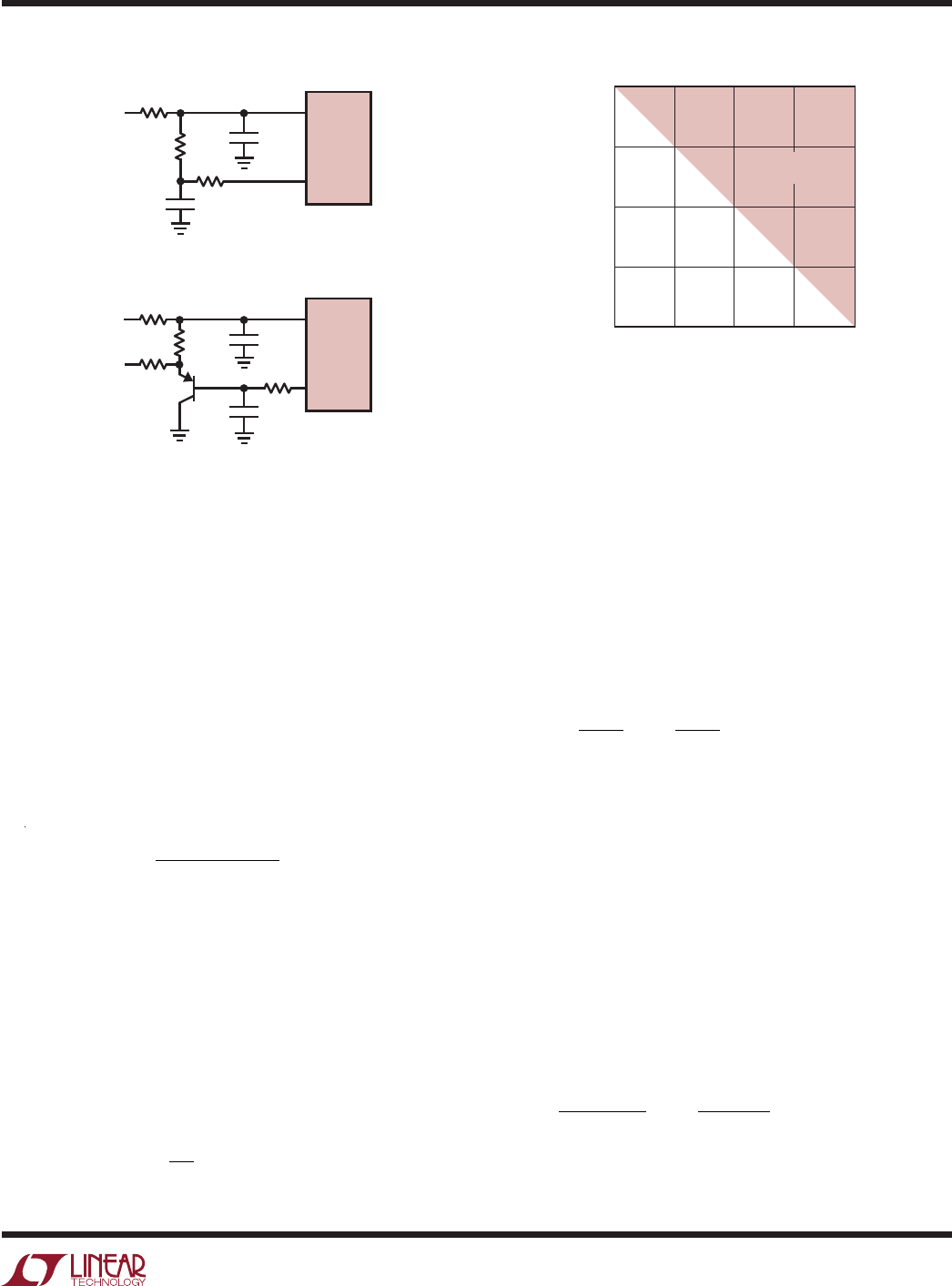
A plot of Maximum Duty Cycle vs Frequency is shown in
Figure 3.
Setting
the Output Voltage
The LTC3608 develops a 0.6V reference voltage between
the feedback pin, V
FB
, and the signal ground as shown in
Figure 6. The output voltage is set by a resistive divider
according to the following formula:
V
OUT
= 0.6V 1+
R2
R1
⎛
⎝
⎜
⎞
⎠
⎟
To improve the frequency response, a feed forward capaci-
tor C1 may also be used. Great care should be taken to
route the V
FB
line away from noise sources, such as the
inductor or the SW line.
Inductor
Selection
Given the desired input and output voltages, the induc-
tor value and operating frequency determine the ripple
current:
ΔI
L
=
V
OUT
f L
⎛
⎝
⎜
⎞
⎠
⎟
1−
V
OUT
V
IN
⎛
⎝
⎜
⎞
⎠
⎟
Lower ripple current reduces core losses in the inductor,
ESR losses in the output capacitors and output voltage
ripple. Highest efficiency operation is obtained at low
frequency with small ripple current. However, achieving
this requires a large inductor. There is a tradeoff between
component size, efficiency and operating frequency.
A reasonable starting point is to choose a ripple current
that is about 40% of I
OUT(MAX)
. The largest ripple current
occurs at the highest V
IN
. To guarantee that ripple current
does not exceed a specified maximum, the inductance
should be chosen according to:
L =
V
OUT
f ΔI
L(MAX)
⎛
⎝
⎜
⎞
⎠
⎟
1−
V
OUT
V
IN(MAX)
⎛
⎝
⎜
⎞
⎠
⎟
Figure 3. Maximum Switching Frequency vs Duty Cycle
2.0
1.5
1.0
0.5
0
0 0.25 0.50 0.75
3608 F03
1.0
DROPOUT
REGION
DUTY CYCLE (V
OUT
/V
IN
)
SWITCHING FREQUENCY (MHz)
Figure 2. Correcting Frequency Shift with Load Current Changes
C
VON
0.01µF
R
VON2
100k
R
VON1
30k
C
C
V
OUT
R
C
(2a)
(2b)
V
ON
I
TH
LTC3608
C
VON
0.01µF
R
VON2
10k
Q1
2N5087
R
VON1
3k
10k
C
C
3608 F02
V
OUT
INTV
CC
R
C
V
ON
I
TH
LTC3608