
Datasheet


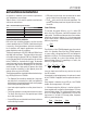


LTC3230
14
3230fa
In 2x boost mode as well, the effi ciency is similar to that
of a linear regulator with an effective input voltage of 2
times the actual input voltage. In an ideal 2x charge pump,
the power effi ciency would be given by:
η= = =
P
P
VI
VI
V
V
LED
IN
LED LED
IN IN
LED
IN
•
•• •22
Thermal Management
For higher input voltages and maximum output current,
there can be substantial power dissipation in the LTC3230.
If the junction temperature increases above approximately
150°C the thermal shutdown circuitry will automatically
deactivate the output current sources, charge pump and
both LDOs. To reduce maximum junction temperature,
a good thermal connection to the PC board is recom-
mended. Connecting the Exposed Pad to a ground plane
and maintaining a solid ground plane under the device
will reduce the thermal resistance of the package and PC
board considerably.
Its built-in thermal shutdown circuitry will protect the
LTC3230 from short term transient events. For continu-
ous operation the maximum rated junction temperature
is 125°C. The power dissipated by the device is made up
of three components:
1. The LTC3230 I
VIN
operating current (found in the Elec-
trical Characteristics table) multiplied by V
IN
.
P
Q
= I
Q
• V
IN
2. The sum of the LED currents multiplied by the differ-
ence between V
IN
• Mode and the LED forward voltage
where Mode is 1, 1.5 or 2 depending on the charge
pump mode.
P
CP
= (V
IN
• Mode – V
LED
) • I
LEDTOTAL
3. For each LDO, the product of the LDO output current
and the difference between V
IN
and the LDO.
P
LDO
= (V
IN
– V
LDO1
) • I
LDO1
+ (V
IN
– V
LDO2
) • I
LDO2
Given a thermal resistance, θ
JA
, for the LTC3230 QFN
package of 68°C/W, at an ambient temperature of 70°C
the total power in the LTC3230 should be kept to less than
815mW. Applications in which the LDO output voltages
are set to the lower range and which use a high V
IN
input
voltage may require limiting the total current output to
keep T
J
less than 125°C at the upper ambient temperature
corners.
An example using the parameters in Table 4 shows an ap-
plication that just meets the maximum junction temperature
limit. An increase in V
IN
, for example, will require reducing
the output current of the charge pump or LDO.
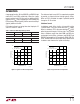
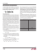
Table 4. T
J
Calculation Example Parameters
V
IN
3.6V
Mode 1.5x
V
LED
3.3V
I
LEDTOTAL
100mA (20mA/LED)
V
LDO1
1.5V
V
LDO2
2.8V
I
LDO1
200mA
I
LDO2
200mA
θ
JA
68°C/W
T
A
70°C
Total Power Dissipation 799mW
Internal Junction Temperature 124°C
APPLICATIONS INFORMATION