
Datasheet


LTC3230
13
3230fa
APPLICATIONS INFORMATION
of capacitor is needed to ensure minimum capacitances
at all temperatures and voltages.
Table 3 shows a list of ceramic capacitor manufacturers
and how to contact them.
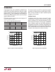
Table 3. Recommended Capacitor Vendors
AVX xww.avxcrp.com
Kemet www.kemet.com
Murata www.murata.com
Taiyo Yuden www.t-yuden.com
Vishay www.vishay.com
Layout Considerations and Noise
Due to the high switching frequency and the transient
currents produced by the LTC3230, careful board layout
is necessary. A true ground plane and short connections
to all capacitors will improve performance and ensure
proper regulation under all conditions.
The fl ying capacitor pins C1P, C2P, C1M and C2M will have
high edge rate waveforms. The large dv/dt on these pins
can couple energy to adjacent PCB runs. Magnetic fi elds
can also be generated if the fl ying capacitors are not close
to the LTC3230 (i.e., the loop area is large). To decouple
capacitive energy transfer, a grounded PCB trace between
the sensitive node and the LTC3230 pins will shield the
sensitive node. For a high quality AC ground, the shield
trace should be returned to a solid ground plane that
extends all the way to the LTC3230.
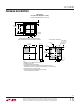
The following guidelines should be followed when design-
ing a PCB layout for the LTC3230:
• The Exposed Pad should be soldered to a large cop-
per plane that is connected to a solid, low impedance
ground plane using plated through hole vias for proper
heat sinking and noise protection.
• Input and output capacitors must be placed close to
the part.
• The fl ying capacitors must be placed close to the part.
The traces from the pins to the capacitor pad should
be as wide as possible.
• V
IN
and CPO traces must be wide to minimize inductance
and handle high currents.
• LED pads must be large and connected to the other
layers of metal to ensure proper heat sinking.
• The R
SET
pin is sensitive to noise and capacitance. The
resistor should be placed near the part with minimum
line width.
Power Effi ciency
To calculate the power effi ciency (η) of a white LED
driver chip, the LED power should be compared to the
input power. The difference between these two numbers
represents lost power whether it is in the charge pump
or the current sources. Stated mathematically, the power
effi ciency is given by:
η=
P
P
LED
IN
The effi ciency of the LTC3230 depends upon the mode in
which it is operating. Recall that the LTC3230 operates
as a pass switch, connecting V
IN
to CPO, until dropout is
detected at a LED pin. This feature provides the optimum
effi ciency available for a given input voltage and LED
forward voltage. When it is operating as a switch, the
effi ciency is approximated by:
η= = =
P
P
VI
VI
V
V
LED
IN
LED LED
IN IN
LED
IN
•
•
since the input current will be very close to the sum of
the LED currents.
At moderate to high output power, the quiescent current
of the LTC3230 is negligible and the expression above is
valid.
Once dropout is detected at any LED pin, the LTC3230
enables the charge pump in 1.5x mode.
In 1.5x boost mode, the effi ciency is similar to that of a
linear regulator with an effective input voltage of 1.5 times
the actual input voltage. This is because the input current
for a 1.5x charge pump is approximately 1.5 times the
load current. In an ideal 1.5x charge pump, the power
effi ciency would be given by:
η= = =
P
P
VI
VI
V
V
LED
IN
LED LED
IN IN
LED
IN
•
•.• .•15 15