
Datasheet


LTC2240-12
21
224012fd
APPLICATIONS INFORMATION
Data Format
The LTC2240-12 parallel digital output can be selected
for offset binary or 2’s complement format. The format
is selected with the MODE pin. Connecting MODE to GND
or 1/3V
DD
selects offset binary output format. Connecting
MODE to 2/3V
DD
or V
DD
selects 2’s complement output
format. An external resistor divider can be used to set the
1/3V
DD
or 2/3V
DD
logic values. Table 3 shows the logic
states for the MODE pin.
Table 3. MODE Pin Function
MODE PIN OUTPUT FORMAT
CLOCK DUTY
CYCLE STABILIZER
GND Offset Binary Off
1/3V
DD
Offset Binary On
2/3V
DD
2’s Complement On
V
DD
2’s Complement Off
Overfl ow Bit
An overfl ow output bit indicates when the converter is
overranged or underranged. In CMOS mode, a logic high
on the OFA pin indicates an overfl ow or underfl ow on the
A data bus, while a logic high on the OFB pin indicates an
overfl ow or underfl ow on the B data bus. In LVDS mode,
a differential logic high on the OF
+
/OF
–
pins indicates an
overfl ow or underfl ow.
Output Clock
The ADC has a delayed version of the ENC
+
input available
as a digital output, CLKOUT. The CLKOUT pin can be used
to synchronize the converter data to the digital system.
This is necessary when using a sinusoidal encode. In
all CMOS modes, A bus data will be updated just after
CLKOUTA rises and can be latched on the falling edge of
CLKOUTA. In demux CMOS mode with interleaved update,
B bus data will be updated just after CLKOUTB rises and
can be latched on the falling edge of CLKOUTB. In demux
CMOS mode with simultaneous update, B bus data will be
updated just after CLKOUTB falls and can be latched on
the rising edge of CLKOUTB. In LVDS mode, data will be
updated just after CLKOUT
+
/CLKOUT
–
rises and can be
latched on the falling edge of CLKOUT
+
/CLKOUT
–
.
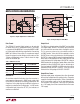
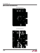
Output Driver Power
Separate output power and ground pins allow the output
drivers to be isolated from the analog circuitry. The power
supply for the digital output buffers, OV
DD
, should be tied
to the same power supply as for the logic being driven.
For example if the converter is driving a DSP powered
by a 1.8V supply then OV
DD
should be tied to that same
1.8V supply.
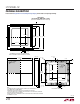
Figure 13a. Digital Output Buffer in CMOS Mode
Figure 13b. Digital Output in LVDS Mode
LTC2240-12
224012 F13a
OV
DD
V
DD
V
DD
0.1μF
43Ω
TYPICAL
DATA
OUTPUT
OGND
OV
DD
0.5V
TO 2.625V
PREDRIVER
LOGIC
DATA
FROM
LATCH
OE
LTC2240-12
224012 F13b
OV
DD
LVDS
RECEIVER
OGND
1.25V
D
D
D
D
OUT
+
0.1μF
2.5V
OUT
–
100Ω
+
–
3.5mA
10k 10k