
Datasheet


LTC2240-12
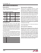
17
224012fd
APPLICATIONS INFORMATION
wideband noise at the converter input. For input frequen-
cies higher than 100MHz, the capacitor may need to be
decreased to prevent excessive signal loss.
The A
IN
+
and A
IN
–
inputs each have two pins to reduce
package inductance. The two A
IN
+
and the two A
IN
–
pins
should be shorted together.
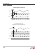
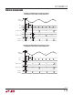
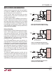
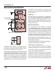
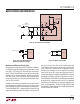
For input frequencies above 100MHz the input circuits of
Figure 6, 7 and 8 are recommended. The balun transformer
gives better high frequency response than a fl ux coupled
center tapped transformer. The coupling capacitors allow
the analog inputs to be DC biased at 1.25V. In Figure 8 the
series inductors are impedance matching elements that
maximize the ADC bandwidth.
Reference Operation
Figure 9 shows the LTC2240-12 reference circuitry consist-
ing of a 1.25V bandgap reference, a difference amplifi er
and switching and control circuit. The internal voltage
reference can be confi gured for two pin selectable input
ranges of 2V (±1V differential) or 1V (±0.5V differential).
Tying the SENSE pin to V
DD
selects the 2V range; typing
the SENSE pin to V
CM
selects the 1V range.
The 1.25V bandgap reference serves two functions: its
output provides a DC bias point for setting the common
mode voltage of any external input circuitry; additionally,
the reference is used with a difference amplifi er to gener-
ate the differential reference levels needed by the internal
ADC circuitry. An external bypass capacitor is required
for the 1.25V reference output, V
CM
. This provides a high
frequency low impedance path to ground for internal and
external circuitry.
The difference amplifi er generates the high and low
reference for the ADC. High speed switching circuits are
connected to these outputs and they must be externally
bypassed. Each output has four pins: two each of REFHA
and REFHB for the high reference and two each of REFLA
Figure 6. Recommended Front End Circuit for
Input Frequencies Between 100MHz and 250MHz
Figure 7. Recommended Front End Circuit for
Input Frequencies Between 250MHz and 500MHz
Figure 8. Recommended Front End Circuit for
Input Frequencies Above 500MHz
25Ω
25Ω
12Ω
12Ω
10Ω
0.1μF
A
IN
+
A
IN
+
A
IN
–
A
IN
–
8pF
2.2μF
V
CM
ANALOG
INPUT
0.1μF
0.1μF
T1
T1 = MA/COM ETC1-1-13
RESISTORS, CAPACITORS
ARE 0402 PACKAGE SIZE
224012 F06
LTC2240-12
25Ω
10Ω
25Ω
0.1μF
A
IN
+
A
IN
+
A
IN
–
A
IN
–
2.2μF
V
CM
ANALOG
INPUT
0.1μF
0.1μF
T1
T1 = MA/COM ETC1-1-13
RESISTORS, CAPACITORS
ARE 0402 PACKAGE SIZE
224012 F07
LTC2240-12
25Ω
10Ω
25Ω
0.1μF
A
IN
+
A
IN
+
A
IN
–
A
IN
–
2.2μF
V
CM
LTC2240-12
ANALOG
INPUT
0.1μF
0.1μF
T1
T1 = MA/COM ETC1-1-13
RESISTORS, CAPACITORS
ARE 0402 PACKAGE SIZE
224012 F08
2.7nH
2.7nH