
Datasheet


LTC2240-12
16
224012fd
APPLICATIONS INFORMATION
Input Drive Impedance
As with all high performance, high speed ADCs, the dy-
namic performance of the LTC2240-12 can be infl uenced
by the input drive circuitry, particularly the second and
third harmonics. Source impedance and input reactance
can infl uence SFDR. At the falling edge of ENC, the sample-
and-hold circuit will connect the 2pF sampling capacitor to
the input pin and start the sampling period. The sampling
period ends when ENC rises, holding the sampled input on
the sampling capacitor. Ideally the input circuitry should be
fast enough to fully charge the sampling capacitor during
the sampling period 1/(2f
S
); however, this is not always
possible and the incomplete settling may degrade the SFDR.
The sampling glitch has been designed to be as linear as
possible to minimize the effects of incomplete settling.
For the best performance, it is recommended to have a
source impedance of 100Ω or less for each input. The
source impedance should be matched for the differential
inputs. Poor matching will result in higher even order
harmonics, especially the second.
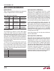
Input Drive Circuits
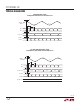
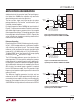
Figure 3 shows the LTC2240-12 being driven by an RF
transformer with a center tapped secondary. The secondary
center tap is DC biased with V
CM
, setting the ADC input
signal at its optimum DC level. Terminating on the trans-
former secondary is desirable, as this provides a common
mode path for charging glitches caused by the sample and
hold. Figure 3 shows a 1:1 turns ratio transformer. Other
turns ratios can be used if the source impedance seen
by the ADC does not exceed 100Ω for each ADC input.
A disadvantage of using a transformer is the loss of low
frequency response. Most small RF transformers have
poor performance at frequencies below 1MHz.
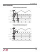
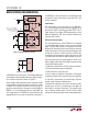
Figure 4 demonstrates the use of a differential amplifi er to
convert a single ended input signal into a differential input
signal. The advantage of this method is that it provides
low frequency input response; however, the limited gain
bandwidth of most op amps will limit the SFDR at high
input frequencies.
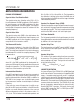
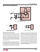
Figure 5 shows a capacitively-coupled input circuit. The
impedance seen by the analog inputs should be matched.
The 25Ω resistors and 12pF capacitor on the analog inputs
serve two purposes: isolating the drive circuitry from
the sample-and-hold charging glitches and limiting the
Figure 3. Single-Ended to Differential
Conversion Using a Transformer
Figure 4. Differential Drive with an Amplifi er
Figure 5. Capacitively-Coupled Drive
25Ω
25Ω
25Ω
25Ω
10Ω
0.1μF
A
IN
+
A
IN
+
A
IN
–
A
IN
–
12pF
2.2μF
V
CM
LTC2240-12
ANALOG
INPUT
0.1μFT1
1:1
T1 = MA/COM ETC1-1T
RESISTORS, CAPACITORS
ARE 0402 PACKAGE SIZE
224012 F03
25Ω
25Ω
50Ω
A
IN
+
A
IN
+
A
IN
–
A
IN
–
12pF
2.2μF
3pF
V
CM
LTC2240-12
224012 F04
–
–
+
+
CM
ANALOG
INPUT
HIGH SPEED
DIFFERENTIAL
AMPLIFIER
3pF
0.1μF
25Ω
0.1μF
V
CM
A
IN
+
A
IN
+
A
IN
–
A
IN
–
100Ω 100Ω
ANALOG
INPUT
12pF
224012 F05
2.2μF
0.1μF
25Ω
LTC2240-12