
Datasheet


8
LTC1872B
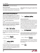
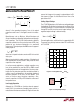
Figure 5. Setting Output Voltage
3
V
FB
V
OUT
LTC1872B
R1
1872B F05
R2
APPLICATIONS INFORMATION
WUU
U
amount of change as the supply is reduced down to 2V.
Also shown in Figure 4 is the effect of V
IN
on V
REF
as V
IN
goes below 2.3V.
Setting Output Voltage
The LTC1872B develops a 0.8V reference voltage between
the feedback (Pin 3) terminal and ground (see Figure 5). By
selecting resistor R1, a constant current is caused to flow
through R1 and R2 to set the overall output voltage. The
regulated output voltage is determined by:
VV
R
R
OUT
=+
08 1
2
1
.
For most applications, an 80k resistor is suggested for R1.
To prevent stray pickup, locate resistors R1 and R2 close
to LTC1872B.
∆VI
VV
V
I
ESR
fC
OUT O
OUT D
IN
RIPPLE
OUT
ť
+
+
•
+
2
1
2
2
2
1
2
π
where f is the operating frequency, C
OUT
is the output
capacitance and I
RIPPLE
is the ripple current in the induc-
tor.
Manufacturers such as Nichicon, United Chemicon and
Sanyo should be considered for high performance through-
hole capacitors. The OS-CON semiconductor dielectric
capacitor available from Sanyo has the lowest ESR (size)
product of any aluminum electrolytic at a somewhat
higher price. The output capacitor RMS current is approxi-
mately equal to:
IDCDC
PK
•−
2
where I
PK
is the peak inductor current and DC is the switch
duty cycle.
When using electrolytic output capacitors, if the ripple and
ESR requirements are met, there is likely to be far more
capacitance than required.
In surface mount applications, multiple capacitors may
have to be paralleled to meet the ESR or RMS current
handling requirements of the application. Aluminum elec-
trolytic and dry tantalum capacitors are both available in
surface mount configurations. An excellent choice of
tantalum capacitors is the AVX TPS and KEMET T510
series of surface mount tantalum capacitors. Also,
ceramic capacitors in X5R pr X7R dielectrics offer excel-
lent performance.
Low Supply Operation
Although the LTC1872B can function down to approxi-
mately 2.0V, the maximum allowable output current is
reduced when V
IN
decreases below 3V. Figure 4 shows the
Figure 4. Line Regulation of V
REF
and V
ITH
INPUT VOLTAGE (V)
2.0
NORMALIZED VOLTAGE (%)
105
100
95
90
85
80
75
2.2 2.4 2.6 2.8
1872B F04
3.0
V
REF
V
ITH