
Datasheet


4
LTC1872B
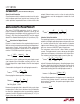
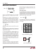
FUNCTIONAL DIAGRA
UU
W
OPERATIO
U
(Refer to Functional Diagram)
Main Control Loop
The LTC1872B is a constant frequency current mode
switching regulator. During normal operation, the external
N-channel power MOSFET is turned on each cycle by the
oscillator and turned off when the current comparator
(ICMP) resets the RS latch. The peak inductor current at
which ICMP resets the RS latch is controlled by the voltage
on the I
TH
/RUN pin, which is the output of the error
amplifier EAMP. An external resistive divider connected
between V
OUT
and ground allows the EAMP to receive an
output feedback voltage V
FB
. When the load current in-
creases, it causes a slight decrease in V
FB
relative to the
0.8V reference, which in turn causes the
I
TH
/RUN voltage to increase until the average inductor
current matches the new load current.
The main control loop is shut down by pulling the I
TH
/RUN
pin low. Releasing I
TH
/RUN allows an internal 0.5µA
current source to charge up the external compensation
network. When the I
TH
/RUN pin reaches 0.35V, the main
control loop is enabled with the I
TH
/RUN voltage then
pulled up to its zero current level of approximately 0.7V.
As the external compensation network continues to charge
up, the corre
sponding output current trip level follows,
allowing normal operation.
Comparator OVP guards against transient overshoots
>7.5% by turning off the external N-channel power
MOSFET and keeping it off until the fault is removed.
Low Load Current Operation
Under very light load current conditions, the I
TH
/RUN pin
voltage will be very close to the zero current level of 0.85V.
As the load current decreases further, an internal offset at
the current comparator input will assure that the current
comparator remains tripped (even at zero load current)
and the regulator will start to skip cycles, as it must, in
order to maintain regulation. This behavior allows the
regulator to maintain constant frequency down to very
light loads, resulting in less low frequency noise genera-
tion over a wide load current range.
SWITCHING
LOGIC AND
BLANKING
CIRCUIT
–
+
–
+
0.5µA
0.3V
OVP
SHDN
1.2V
UV
1872B FD
V
REF
+
60mV
V
REF
0.8V
V
IN
RS
VOLTAGE
REFERENCE
SLOPE
COMP
ICMP
R
S
Q
FREQ
FOLDBACK
OSC
15mV
SENSE
–
V
IN
5
2
4
–
+
4
EAMP
V
FB
–
+
3
NGATE
V
IN
6
I
TH
/RUN
V
IN
0.35V
V
REF
0.8V
1
–
+
SHDN
CMP
GND
–
+
UNDERVOLTAGE
LOCKOUT