
Datasheet
LTC1871
8
1871fe
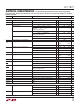
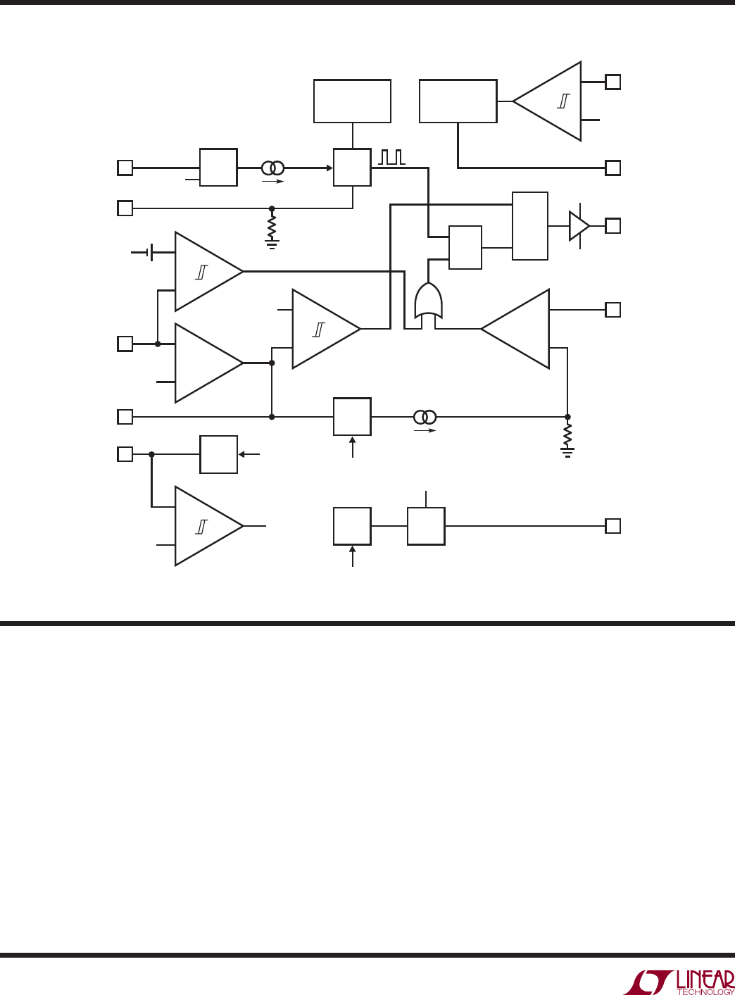
BLOCK DIAGRAM
–
+
–
+
+
1.230V
85mV
OV
50k
EA
UV
TO
START-UP
CONTROL
BURST
COMPARATOR
S
R
Q
LOGIC
PWM LATCH
CURRENT
COMPARATOR
0.30V
1.230V
5.2V
–
+
2.00V
1.230V
SLOPE
1.230V
I
LOOP
FB
I
TH
–
+
g
m
3
MODE/SYNC
5
FREQ
4
2
INTV
CC
8
LDO
V-TO-I
OSCV-TO-I
SLOPE
COMPENSATION
BIAS AND
START-UP
CONTROL
V
IN
BIAS V
REF
I
OSC
R
LOOP
–
+
–
+
C1
SENSE
10
GND
1871 BD
6
GATE
INTV
CC
GND
7
V
IN
1.248V
9
RUN
C2
1
0.6V
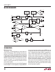
Main Control Loop
The LTC1871 is a constant frequency, current mode con-
troller for DC/DC boost, SEPIC and fl yback converter ap-
plications. The LTC1871 is distinguished from conventional
current mode controllers because the current control loop
can be closed by sensing the voltage drop across the power
MOSFET switch instead of across a discrete sense resistor,
as shown in Figure 2. This sensing technique improves
effi ciency, increases power density, and reduces the cost
of the overall solution.
For circuit operation, please refer to the Block Diagram of
the IC and Figure 1. In normal operation, the power MOSFET
is turned on when the oscillator sets the PWM latch and
is turned off when the current comparator C1 resets the
latch. The divided-down output voltage is compared to an
internal 1.230V reference by the error amplifi er EA, which
outputs an error signal at the I
TH
pin. The voltage on the
I
TH
pin sets the current comparator C1 input threshold.
When the load current increases, a fall in the FB voltage
relative to the reference voltage causes the I
TH
pin to rise,
which causes the current comparator C1 to trip at a higher
peak inductor current value. The average inductor current
will therefore rise until it equals the load current, thereby
maintaining output regulation.
OPERATION