
Datasheet
LTC1871
4
1871fe
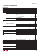
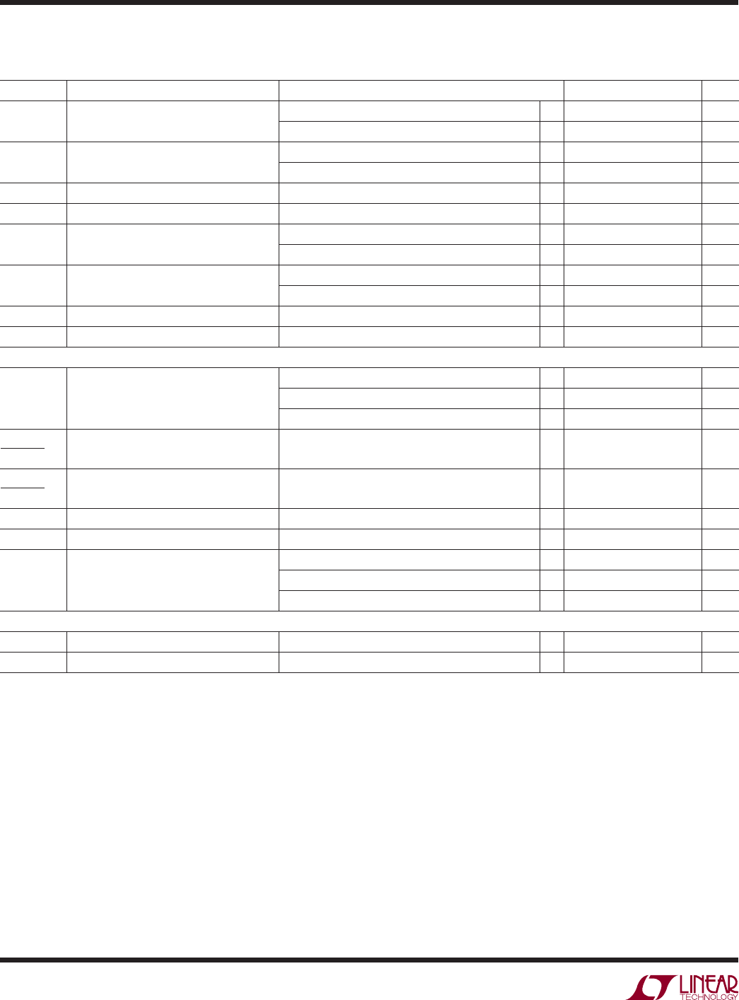
ELECTRICAL CHARACTERISTICS
The l denotes the specifi cations which apply over the full operating
temperature range, otherwise specifi cations are at T
A
= 25°C. V
IN
= V
INTVCC
= 5V, V
RUN
= 1.5V, R
FREQ
= 80k, V
MODE/SYNC
= 0V, unless
otherwise specifi ed.
SYMBOL PARAMETER CONDITIONS MIN TYP MAX UNITS
D
MAX
Maximum Duty Cycle 87 92 97 %
I-Grade or H-Grade (Note 2)
●
87 92 97 %
f
SYNC/
f
OSC
Recommended Maximum Synchronized
Frequency Ratio
f
OSC
= 300kHz (Note 6) 1.25 1.30
f
OSC
= 300kHz (Note 6), I-Grade or H-Grade (Note 2)
●
1.25 1.30
t
SYNC(MIN)
MODE/SYNC Minimum Input Pulse Width V
SYNC
= 0V to 5V 25 ns
t
SYNC(MAX)
MODE/SYNC Maximum Input Pulse Width V
SYNC
= 0V to 5V 0.8/f
OSC
ns
V
IL(MODE)
Low Level MODE/SYNC Input Voltage 0.3 V
I-Grade or H-Grade (Note 2)
●
0.3 V
V
IH(MODE)
High Level MODE/SYNC Input Voltage 1.2 V
I-Grade or H-Grade (Note 2)
●
1.2 V
R
MODE/SYNC
MODE/SYNC Input Pull-Down Resistance 50 k
V
FREQ
Nominal FREQ Pin Voltage 0.62 V
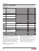
Low Dropout Regulator
V
INTVCC
INTV
CC
Regulator Output Voltage V
IN
= 7.5V 5.0 5.2 5.4 V
V
IN
= 7.5V, I-Grade (Note 2)
●
5.0 5.2 5.4 V
V
IN
= 7.5V, H-Grade (Note 2)
●
4.95 5.2 5.45 V
ΔV
INTVCC
Δ
V
IN1
INTV
CC
Regulator Line Regulation 7.5V ≤ V
IN
≤ 15V 8 25 mV
ΔV
INTVCC
Δ
V
IN2
INTV
CC
Regulator Line Regulation 15V ≤ V
IN
≤ 30V 70 200 mV
V
LDO(LOAD)
INTV
CC
Load Regulation 0 ≤ I
INTVCC
≤ 20mA, V
IN
= 7.5V –2 –0.2 %
V
DROPOUT
INTV
CC
Regulator Dropout Voltage V
IN
= 5V, INTV
CC
Load = 20mA 280 mV
I
INTVCC
Bootstrap Mode INTV
CC
Supply
Current in Shutdown
RUN = 0V, SENSE = 5V 10 20 µA
I-Grade (Note 2)
●
30 µA
H-Grade (Note 2)
●
50 µA
GATE Driver
t
r
GATE Driver Output Rise Time C
L
= 3300pF (Note 7) 17 100 ns
t
f
GATE Driver Output Fall Time C
L
= 3300pF (Note 7) 8 100 ns
Note 1: Stresses beyond those listed under Absolute Maximum Ratings
may cause permanent damage to the device. Exposure to any Absolute
Maximum Rating condition for extended periods may affect device
reliability and lifetime.
Note 2: The LTC1871E is guaranteed to meet performance specifi cations
from 0°C to 85°C operating temperature. Specifi cations over the –40°C to
85°C operating temperature range are assured by design, characterization
and correlation with statistical process controls. The LTC1871I is
guaranteed over the full –40°C to 125°C operating temperature range
and the LTC1871H is guaranteed over the full –40°C to 150°C operating
temperature range.
Note 3: T
J
is calculated from the ambient temperature T
A
and power
dissipation P
D
according to the following formula:
T
J
= T
A
+ (P
D
• 110°C/W)
Note 4: The dynamic input supply current is higher due to power MOSFET
gate charging (Q
G
• f
OSC
). See Applications Information.
Note 5: The LTC1871 is tested in a feedback loop which servos V
FB
to
the reference voltage with the I
TH
pin forced to the midpoint of its voltage
range (0.3V ≤ V
ITH
≤ 1.2V, midpoint = 0.75V).
Note 6: In a synchronized application, the internal slope compensation
gain is increased by 25%. Synchronizing to a signifi cantly higher ratio will
reduce the effective amount of slope compensation, which could result in
subharmonic oscillation for duty cycles greater than 50%.
Note 7: Rise and fall times are measured at 10% and 90% levels.