
Datasheet
LTC1871
24
1871fe
APPLICATIONS INFORMATION
that the input fi lter capacitor for the LTC1871 is not
shared with other converters. AC input current from
another converter could cause substantial input voltage
ripple, and this could interfere with the operation of the
LTC1871. A few inches of PC trace or wire (L ≈ 100nH)
between the C
IN
of the LTC1871 and the actual source
V
IN
should be suffi cient to prevent current sharing
problems.
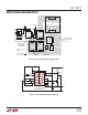
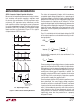
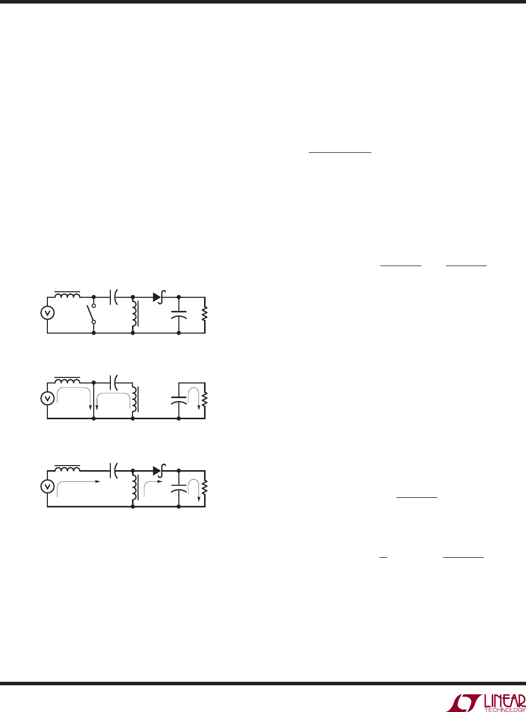
SEPIC Converter Applications
The LTC1871 is also well suited to SEPIC (single-ended
primary inductance converter) converter applications. The
SEPIC converter shown in Figure 16 uses two inductors.
The advantage of the SEPIC converter is the input voltage
may be higher or lower than the output voltage, and the
output is short-circuit protected.
Figures 16. SEPIC Topology and Current Flow
+
+
+
•
•
•
•
SW L2
C
OUT
R
L
V
OUT
V
IN
C1
D1
L1
16a. SEPIC Topology
+
+
+
•
R
L
V
OUT
V
IN
D1
16c. Current Flow During Switch Off-Time
+
+
+
•
R
L
V
OUT
V
IN
V
IN
V
IN
16b. Current Flow During Switch On-Time
The fi rst inductor, L1, together with the main switch,
resembles a boost converter. The second inductor, L2,
together with the output diode D1, resembles a fl yback or
buck-boost converter. The two inductors L1 and L2 can be
independent but can also be wound on the same core since
identical voltages are applied to L1 and L2 throughout the
switching cycle. By making L1 = L2 and winding them on
the same core the input ripple is reduced along with cost
and size. All of the SEPIC applications information that
follows assumes L1 = L2 = L.
SEPIC Converter: Duty Cycle Considerations
For a SEPIC converter operating in a continuous conduction
mode (CCM), the duty cycle of the main switch is:
D=
V
O
+ V
D
V
IN
+ V
O
+ V
D
where V
D
is the forward voltage of the diode. For convert-
ers where the input voltage is close to the output voltage
the duty cycle is near 50%.
The maximum output voltage for a SEPIC converter is:
V
O(MAX)
= V
IN
+ V
D
()
D
MAX
1–D
MAX
–V
D
1
1–D
MAX
The maximum duty cycle of the LTC1871 is typically
92%.
SEPIC Converter: The Peak and Average Input
Currents
The control circuit in the LTC1871 is measuring the input
current (either using the R
DS(ON)
of the power MOSFET
or by means of a sense resistor in the MOSFET source),
so the output current needs to be refl ected back to the
input in order to dimension the power MOSFET properly.
Based on the fact that, ideally, the output power is equal
to the input power, the maximum input current for a SEPIC
converter is:
I
IN(MAX)
= I
O(MAX)
•
D
MAX
1–D
MAX
The peak input current is:
I
IN(PEAK)
= 1+
2
•I
O(MAX)
•
D
MAX
1–D
MAX
The maximum duty cycle, D
MAX
, should be calculated at
minimum V
IN
.
The constant ‘χ’ represents the fraction of ripple current in
the inductor relative to its maximum value. For example, if
30% ripple current is chosen, then χ = 0.30 and the peak
current is 15% greater than the average.