
Datasheet
LTC1871
21
1871fe
APPLICATIONS INFORMATION
A second, more severe transient can occur when con-
necting loads with large (>1µF) supply bypass capacitors.
The discharged bypass capacitors are effectively put in
parallel with C
O
, causing a nearly instantaneous drop in
V
O
. No regulator can deliver enough current to prevent
this problem if the load switch resistance is low and it is
driven quickly. The only solution is to limit the rise time
of the switch drive in order to limit the inrush current
di/dt to the load.
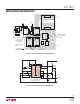
Boost Converter Design Example
The design example given here will be for the circuit shown
in Figure 1. The input voltage is 3.3V, and the output is 5V
at a maximum load current of 7A (10A peak).
1. The duty cycle is:
D=
V
O
+ V
D
–V
IN
V
O
+ V
D
=
5 + 0.4 – 3.3
5 +
0.4
= 38.9%
2. Pulse-skip operation is chosen so the MODE/SYNC pin
is shorted to INTV
CC
.
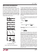
3. The operating frequency is chosen to be 300kHz to
reduce the size of the inductor. From Figure 5, the
resistor from the FREQ pin to ground is 80k.
4. An inductor ripple current of 40% of the maximum load
current is chosen, so the peak input current (which is
also the minimum saturation current) is:
I
IN(PEAK)
= 1+
2
•
I
O(MAX)
1–D
MAX
= 1.2 •
7
1– 0.39
= 13.8A
The inductor ripple current is:
I
L
= •
I
O(MAX)
1–D
MAX
= 0.4 •
7
1–
0.39
= 4.6A
And so the inductor value is:
L =
V
IN(MIN)
I
L
• f
•D
MAX
=
3.3V
4.6A • 300kHz
• 0.39 = 0.93μH
The component chosen is a 1µH inductor made by
Sumida (part number CEP125-H 1ROMH) which has
a saturation current of greater than 20A.
5. With the input voltage to the IC bootstrapped to the
output of the power supply (5V), a logic-level MOSFET
can be used. Because the duty cycle is 39%, the maxi-
mum SENSE pin threshold voltage is reduced from its
low duty cycle typical value of 150mV to approximately
140mV. Assuming a MOSFET junction temperature of
125°C, the room temperature MOSFET R
DS(ON)
should
be less than:
R
DS(ON)
V
SENSE(MAX)
•
1–D
MAX
1+
2
•I
O(MAX)
•
T
= 0.140V •
1– 0.39
1+
0.4
2
•7A•
1.5
= 6.8m
The MOSFET used was the Fairchild FDS7760A, which
has a maximum R
DS(ON)
of 8m at 4.5V V
GS
, a BV
DSS
of greater than 30V, and a gate charge of 37nC at 5V
V
GS
.
6. The diode for this design must handle a maximum
DC output current of 10A and be rated for a minimum
reverse voltage of V
OUT
, or 5V. A 25A, 15V diode from
On Semiconductor (MBRB2515L) was chosen for its
high power dissipation capability.
7. The output capacitor usually consists of a high valued
bulk C connected in parallel with a lower valued, low
ESR ceramic. Based on a maximum output ripple voltage
of 1%, or 50mV, the bulk C needs to be greater than:
C
OUT
I
OUT(MAX)
0.01• V
OUT
• f
=
7A
0.01• 5V • 300kH
z
= 466μF
The RMS ripple current rating for this capacitor needs
to exceed:
I
RMS(COUT)
I
O(MAX)
•
V
O
–V
IN(MIN)
V
IN(MIN)
=
7A •
5V – 3.3V
3.3
V
= 5A
To satisfy this high RMS current demand, four
150µF Panasonic capacitors (EEFUEOJ151R) are
required. In parallel with these bulk capacitors, two
22µF, low ESR (X5R) Taiyo Yuden ceramic capacitors