
Datasheet

LTC1871
20
1871fe
APPLICATIONS INFORMATION
then off, a packet of gate charge Q
G
is transferred from
INTV
CC
to ground. The resulting dQ/dt is a current that
must be supplied to the INTV
CC
capacitor through the
V
IN
pin by an external supply. If the IC is operating in
CCM:
I
Q(TOT)
≈ I
Q
= f • Q
G
P
IC
= V
IN
• (I
Q
+ f • Q
G
)
2. Power MOSFET switching and conduction losses. The
technique of using the voltage drop across the power
MOSFET to close the current feedback loop was chosen
because of the increased effi ciency that results from
not having a sense resistor. The losses in the power
MOSFET are equal to:
P
FET
=
I
O(MAX)
1–D
MAX
2
•R
DS(ON)
•D
MAX
•
T
+k•V
O
1.85
•
I
O(MAX)
1–D
MAX
( )
•C
RSS
•f
The I
2
R power savings that result from not having a
discrete sense resistor can be calculated almost by
inspection.
P
R(SENSE)
=
I
O(MAX)
1–D
MAX
2
•R
SENSE
•D
MAX
To understand the magnitude of the improvement with
this V
DS
sensing technique, consider the 3.3V input,
5V output power supply shown in Figure 1. The maxi-
mum load current is 7A (10A peak) and the duty cycle
is 39%. Assuming a ripple current of 40%, the peak
inductor current is 13.8A and the average is 11.5A.
With a maximum sense voltage of about 140mV, the
sense resistor value would be 10m, and the power
dissipated in this resistor would be 514mW at maxi-
mum output current. Assuming an effi ciency of 90%,
this sense resistor power dissipation represents 1.3%
of the overall input power. In other words, for this ap-
plication, the use of V
DS
sensing would increase the
effi ciency by approximately 1.3%.
For more details regarding the various terms in these
equations, please refer to the section Boost Converter:
Power MOSFET Selection.
3. The losses in the inductor are simply the DC input cur-
rent squared times the winding resistance. Expressing
this loss as a function of the output current yields:
P
R(WINDING)
=
I
O(MAX)
1–D
MAX
2
•R
W
4. Losses in the boost diode. The power dissipation in the
boost diode is:
P
DIODE
= I
O(MAX)
• V
D
The boost diode can be a major source of power loss
in a boost converter. For the 3.3V input, 5V output at
7A example given above, a Schottky diode with a 0.4V
forward voltage would dissipate 2.8W, which represents
7% of the input power. Diode losses can become signifi -
cant at low output voltages where the forward voltage
is a signifi cant percentage of the output voltage.
5. Other losses, including C
IN
and C
O
ESR dissipation and
inductor core losses, generally account for less than
2% of the total additional loss.
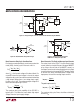
Checking Transient Response
The regulator loop response can be verifi ed by looking at
the load transient response. Switching regulators generally
take several cycles to respond to an instantaneous step
in resistive load current. When the load step occurs, V
O
immediately shifts by an amount equal to (ΔI
LOAD
)(ESR),
and then C
O
begins to charge or discharge (depending on
the direction of the load step) as shown in Figure 13. The
regulator feedback loop acts on the resulting error amp
output signal to return V
O
to its steady-state value. During
this recovery time, V
O
can be monitored for overshoot or
ringing that would indicate a stability problem.
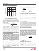
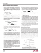
Figure 13. Load Transient Response for a 3.3V Input,
5V Output Boost Converter Application, 0.7A to 7A Step
I
OUT
2V/DIV
V
OUT
(AC)
100mV/DIV
100µs/DIV
1871 F13
V
IN
= 3.3V
V
OUT
= 5V
MODE/SYNC = INTV
CC
(PULSE-SKIP MODE)